


Next: 2.5 Achievable Lower Bounds
Up: 2.4 Absolute Lower Bounds
Previous: 2.4.1 Lower Bound of
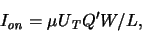
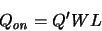
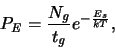
To determine a lower bound for the switching energy we regard
only the intrinsic channel charge of a turned-on transistor
(still operating in weak inversion). With
 |
(2.16) |
 |
(2.17) |
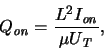
the channel charge becomes
 |
(2.18) |
where L is the effective channel length and  is the effective
carrier mobility, and the turn-on current
is the effective
carrier mobility, and the turn-on current
 for a given
supply voltage is adjusted by the channel doping.
If we now consider an inverter chain with each output node connected
to the two gates of the following stage, and we neglect all other
parasitics, then the charge of this node is altered by
for a given
supply voltage is adjusted by the channel doping.
If we now consider an inverter chain with each output node connected
to the two gates of the following stage, and we neglect all other
parasitics, then the charge of this node is altered by
 during one clock period, so that the switching energy is given by
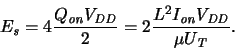 |
(2.19) |
This means that the mere device physics does not limit the switching
energy, because
can be chosen almost arbitrarily (disregarding
design rules and tunneling effects).
However, if we require a node to be charged with
at least, say, 10 electrons then (taking
 for
for
 from
Table 2.2) the switching energy is at least 0.13aJ.
Another limit comes from the error rate in digital systems
subject to thermal noise [75]
from
Table 2.2) the switching energy is at least 0.13aJ.
Another limit comes from the error rate in digital systems
subject to thermal noise [75]
 |
(2.20) |
where
 is the number of gates and
 is
the gate delay which is larger than the inverter delay
is
the gate delay which is larger than the inverter delay
 |
(2.21) |
If we assume, e.g., a deep sub-micron technology with  and
and
 ,
and a system with 107 gates
requiring less than one error per year, then we get
,
and a system with 107 gates
requiring less than one error per year, then we get
 and
and
 .
.
Of course, these values cannot be reached because of the parasitics, most
important the gate-drain overlap, junction, and interconnect
capacitances, that were not accounted for. When these are included the
circuit speed becomes a function of
,
making higher currents
necessary to keep up the performance and they also add to the
switching energy by
 .
Because the parasitics are largely technology dependent a simple
general analysis is not possible. However, what can be seen
from (2.19) is that the power efficiency scales as 1/L2,
i.e., the benefit of ULP CMOS increases with down-scaling.
.
Because the parasitics are largely technology dependent a simple
general analysis is not possible. However, what can be seen
from (2.19) is that the power efficiency scales as 1/L2,
i.e., the benefit of ULP CMOS increases with down-scaling.
Heisenberg's uncertainty principle does not impose a lower bound
on the switching energy but actually another tradeoff between
speed and energy
[26,45,46]:2.1
 |
(2.22) |
Footnotes
- ...A0248,R0069,K0134:2.1
-
For
 the minimum energy would be
 .
.
Next: 2.5 Achievable Lower Bounds
Up: 2.4 Absolute Lower Bounds
Previous: 2.4.1 Lower Bound of
G. Schrom