next up previous contents
Next: 3.3.6 Power Consumption Up: 3.3 VLSI Performance Metric Previous: 3.3.4 Key Parameters and


3.3.5 Dynamic Inverter Model

The inverter delay $\ensuremath{t_{\mathit{d}}}\xspace $ is determined by the drive current $\ensuremath{I_{\mathit{on}}}\xspace $, $\ensuremath{V_{\mathit{DD}}}\xspace $, the non-linear capacitances of the intrinsic transistors, and the interconnect capacitances. 
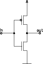
The capacitances are modeled into a single load capacitance at the inverter output (cf. Fig. 3.5 and (3.20)).

Figure 3.5: Dynamic inverter model
\includegraphics{inverter.ps}
\includegraphics[scale=0.4]{invmod.eps}

The influence of the non-linear capacitances can also be formulated as follows: For switching one transistor a total switching charge of

\begin{displaymath}
\renewcommand {1.20}{1.6}
\begin{array}{rcl}
\ensuremat...
...}}\xspace (\ensuremath{V_{\mathit{DD}}}\xspace )
\end{array}\end{displaymath} (3.19)

is transferred. The charges can be obtained as a function of $\ensuremath{V_{\mathit{DD}}}\xspace $ from two transient simulations (3a, 3b) as shown in Fig. 3.6 [64]. The trajectory used to determine the charges (solid line) is different from the actual switching trajectory (dashed line), which is justified by the quasi-static model. The switching charge $\ensuremath{Q_{\mathit{sw}}}\xspace $ covers automatically all parasitic capacitances of the simulated device structure.

Figure 3.6: Transient determination of the switching charge $\ensuremath{Q_{\mathit{sw}}}\xspace $
\includegraphics[scale=0.5]{qsw-idea.eps}
\includegraphics[scale=0.5]{qsw-simx.eps}

An effective load capacitance $\ensuremath{C_{\mathit{L}}}\xspace $ including interconnects is then determined as

\begin{displaymath}
\ensuremath{C_{\mathit{L}}}\xspace = \frac{\ensuremath{Q_{\...
...ath{c_{\mathit{M}}}\xspace \ensuremath{L_{\mathit{M}}}\xspace
\end{displaymath} (3.20)

and the loaded-inverter delay is estimated as

x
\begin{displaymath}
\ensuremath{t_{\mathit{d}}}\xspace = \frac{\ensuremath{V_{\...
...}}}\xspace - \ensuremath{I_{\mathit{off}}}\xspace )} \cdot k_3
\end{displaymath} (3.21)

Assuming an inverter chain the maximum clock frequency becomes then

x
\begin{displaymath}
\ensuremath{f_{\mathit{c,max}}}\xspace = \frac {1}{\ensuremath{t_{\mathit{d}}}\xspace \ensuremath{{\mathit{ld}}}\xspace }
\end{displaymath} (3.22)

The factors k1 and k2 are used to scale the data of one device to obtain the delay of a CMOS inverter. They account for the average drive current $((\ensuremath{I_{\mathit{on,n}}}\xspace -\ensuremath{I_{\mathit{off,n}}}\xspace...
..._1 (\ensuremath{I_{\mathit{on}}}\xspace -\ensuremath{I_{\mathit{off}}}\xspace )$ and for the effective total capacitance $(\ensuremath{Q_{\mathit{sw,n}}}\xspace +\ensuremath{Q_{\mathit{sw,p}}}\xspace )...
...= k_2 \ensuremath{Q_{\mathit{sw}}}\xspace /\ensuremath{V_{\mathit{DD}}}\xspace $. Typically, for a CMOS inverter with minimum-size transistors these factors are k1 = 0.75 and k2 > 2 for NMOS data.

The empirical correction factor k3 is typically < 1 and accounts for the fact that in a circuit the output nodes start to switch before the input pulse edge is complete. k3 was determined from device-level simulations of a ring oscillator with MINIMOS-NT [72] as follows: setting $k_1=((\ensuremath{I_{\mathit{on,n}}}\xspace -\ensuremath{I_{\mathit{off,n}}}\xs...
...\ensuremath{I_{\mathit{on,n}}}\xspace -\ensuremath{I_{\mathit{off,n}}}\xspace )$ and $k_2=(\ensuremath{Q_{\mathit{sw,n}}}\xspace +\ensuremath{Q_{\mathit{sw,p}}}\xspace )/\ensuremath{Q_{\mathit{sw,n}}}\xspace $, yields $k_3=t_{d,osc}/(k_2\ensuremath{Q_{\mathit{sw}}}\xspace /k_1(\ensuremath{I_{\mathit{on,n}}}\xspace -\ensuremath{I_{\mathit{off,n}}}\xspace ))$, where td,osc is the reference delay time determined from the ring oscillator. Using the devices of Section 3.3.8   k3 was found to be 0.63. The value of k3 does not change much with technology. Evaluating (2.21) with the same value of k3 for a completely different technology (an ultra-low-power technology with Vdd=0.2V [61]) using both NMOS and PMOS data gave an error of -22%.

Although (2.21) and (3.22) are generally not very accurate, they reflect the various tendencies very closely and are therefore well-suited for optimization purposes. Furthermore, the device characterization method which is specific to this approach can be combined with a more detailed system model (cf. [22]) to account for the effect of the particular circuit design style and metalization scheme.

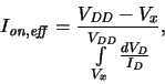
An alternative to using the on-state current directly is to compute an effective turn-on current \ensuremath{I_{\mathit{on,eff}}} from an output curve (4b) as follows:

\begin{displaymath}
\ensuremath{I_{\mathit{on,eff}}}\xspace = {\displaystyle\fr...
...\mathit{D}}}\xspace }{\ensuremath{I_{\mathit{D}}}\xspace }}}}
,\end{displaymath} (3.23)

where Vx is the drain voltage at which the following stage starts to switch; typical values are $\ensuremath{V_{\mathit{DD}}}\xspace /3$- $\ensuremath{V_{\mathit{DD}}}\xspace /2$. Vx can be determined by fitting a CV/I-metric $\ensuremath{t_{\mathit{d}}}\xspace = \ensuremath{C_{\mathit{L}}}\xspace (\ensuremath{V_{\mathit{DD}}}\xspace -V_x)/\ensuremath{I_{\mathit{on,eff}}}\xspace $ to the results obtained from circuit simulations. This approach is in essence equivalent to the one proposed in [5], where an effective equivalent switching resistance $\ensuremath{R_{\mathit{sw}}}\xspace = \int{dV/I}$ is used. The advantage of this method is that the effect of DIBL on the output curve, which is an essential speed degradation effect, is accounted for automatically. Using (3.23) to determine a degradation factor $\ensuremath{I_{\mathit{on,eff}}}\xspace /\ensuremath{I_{\mathit{on}}}\xspace $ has the advantage that this can be done for gate voltages smaller than \ensuremath{V_{\mathit{DD}}}, e.g., for $\ensuremath{V_{\mathit{G}}}\xspace = \ensuremath{V_{\mathit{DD}}}\xspace /2$, which allows the implementation in the performance metric proposed in [65] without further device simulations (in this case the effect of DIBL would be somewhat overestimated). Uncalibrated simulations (i.e., with k3=1) with $V_x = \ensuremath{V_{\mathit{DD}}}\xspace /3$ resulted in delay times with an error of less than 7%.


next up previous contents
Next: 3.3.6 Power Consumption Up: 3.3 VLSI Performance Metric Previous: 3.3.4 Key Parameters and

G. Schrom