


Next: 3.3.8 Application
Up: 3.3 VLSI Performance Metric
Previous: 3.3.6 Power Consumption
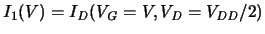
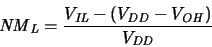
The determination of the static noise margins (cf. Section A.2.2.1)
 ,
,
 would require circuit simulation of an inverter.
A close estimate of the noise margins can be determined from
just two DC simulations (4a, 4b).
Exploiting the fact that the input voltages
would require circuit simulation of an inverter.
A close estimate of the noise margins can be determined from
just two DC simulations (4a, 4b).
Exploiting the fact that the input voltages
 ,
,
 will be
around
will be
around
 and that one of the output transistors is in saturation,
the following algorithm can be used to determine the noise margins:
The currents and conductances at the critical voltages (i.e., where
the inverter gain is
and that one of the output transistors is in saturation,
the following algorithm can be used to determine the noise margins:
The currents and conductances at the critical voltages (i.e., where
the inverter gain is
 )
are estimated by scaling two IV curves
according to Fig. 3.7. With
)
are estimated by scaling two IV curves
according to Fig. 3.7. With
 ,
,
 ,
and
,
and
 the critical voltages
,
the critical voltages
,
 can be obtained by solving:
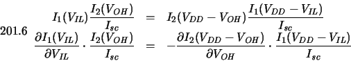 |
(3.27) |
The input-low noise margin
is then
 |
(3.28) |
and the input-high noise margin is determined accordingly
(cf. (A.18)).
In the case of a single-device analysis the inverter transfer curves
are symmetric and the noise margins are
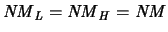 .
The noise margins of gates can be estimated also by scaling the currents
I1, I2 according to the fan-in and the logic style,
e.g., for a static-logic NAND gate with a fan-in of
.
The noise margins of gates can be estimated also by scaling the currents
I1, I2 according to the fan-in and the logic style,
e.g., for a static-logic NAND gate with a fan-in of
 we obtain
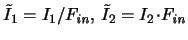 .
Inverter gain and output voltage swing are determined as
.
Inverter gain and output voltage swing are determined as
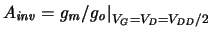 and
and
 from 4a/4b
and 2/5a respectively.
from 4a/4b
and 2/5a respectively.
Figure 3.7:
Determination of static noise margins
![\includegraphics[scale=0.8]{nm-sim.eps}](img471.gif)
|
Next: 3.3.8 Application
Up: 3.3 VLSI Performance Metric
Previous: 3.3.6 Power Consumption
G. Schrom