


Next: A.2.2.3 Transmission Gates, Tri-State
Up: A.2.2 Basic Circuits and
Previous: A.2.2.1 CMOS Inverters
A.2.2.2 Logic Blocks
The series connection of two NMOS switches controlled by the voltages
A and B is conducting only when both A and B
are HIGH. Thus, the series connection implements the logical AND
function, or, the Boolean product
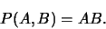 |
(A.19) |
Likewise, a parallel connection of two NMOS switches implements the
logical OR function, or, the Boolean sum
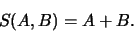 |
(A.20) |
Furthermore, such logical functions can again be combined by series
and parallel connection. This way any boolean expression
of a vector of variables and their complements can be constructed.
The complements
 of the variables xi can be built with
inverters.
An example is shown in Fig. A.7, where a more complex
function F is implemented with a block of NMOS transistors
(note that the function type of such a block is conduction, not voltage).
The dual blockA.1
of PMOS transistors implements the complementary switching function
of the variables xi can be built with
inverters.
An example is shown in Fig. A.7, where a more complex
function F is implemented with a block of NMOS transistors
(note that the function type of such a block is conduction, not voltage).
The dual blockA.1
of PMOS transistors implements the complementary switching function
 ,
i.e., the dual p-block is conducting exactly when the n-block is
not.
Now, a complete CMOS gate can be built by simply connecting the
p-block from
,
i.e., the dual p-block is conducting exactly when the n-block is
not.
Now, a complete CMOS gate can be built by simply connecting the
p-block from
 to the output and the n-block from the output to
ground, like in Fig. A.8,
so that the output voltage is the complement of the
switching function of the n-block:
to the output and the n-block from the output to
ground, like in Fig. A.8,
so that the output voltage is the complement of the
switching function of the n-block:

Figure A.7:
N-block implementation of a Boolean function
|
[Circuit]
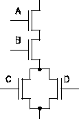
[Boolean switching function]
|
Note, that an n-block must always have a connection to ground
(possibly through other NMOS transistors) because
 must be sufficiently large and positive to turn the transistors on.
For the same reason a p-block must always have a connection to
.
This is one reason why the use of NMOS and PMOS
transistors in the same logic block is unfavorable.
must be sufficiently large and positive to turn the transistors on.
For the same reason a p-block must always have a connection to
.
This is one reason why the use of NMOS and PMOS
transistors in the same logic block is unfavorable.
Figure A.8:
CMOS gate built from an n-block and the dual p-block
|
[Circuit]
![\includegraphics[scale=1.0]{blk-c.ps}](img744.gif)
|
Footnotes
- ... blockA.1
-
A logic block can represented as a graph where each edge corresponds to
a switch. The dual block is constructed by taking the dual graph, i.e., by
replacing series connections with parallel connections and vice
versa.
Next: A.2.2.3 Transmission Gates, Tri-State
Up: A.2.2 Basic Circuits and
Previous: A.2.2.1 CMOS Inverters
G. Schrom