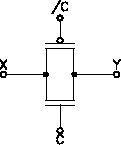
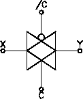
To build a switch that can work from ground to
![]() an NMOS and
a PMOS switch are connected in parallel as shown in Fig. A.9.
When the control signal C is high, at least one of the
transistors connects X and Y (note that also the
complement of C is needed). This circuit is called transmission
gate which can also be used as a switch in analog circuits
(see Section 5.2.1).
an NMOS and
a PMOS switch are connected in parallel as shown in Fig. A.9.
When the control signal C is high, at least one of the
transistors connects X and Y (note that also the
complement of C is needed). This circuit is called transmission
gate which can also be used as a switch in analog circuits
(see Section 5.2.1).
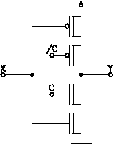
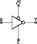
Another circuit which is used to break and make connections
is the tri-state inverter shown in Fig. A.10. When the control
signal C is HIGH the output Y is the inverted input
signal X. Otherwise, when C is LOW, the output is
disconnected (i.e., the so-called high-Z state, which adds to
1 and 0 a third state Z).
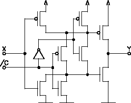
When long lines (interconnects) or chip outputs must be driven
buffer circuits like the one in Fig. A.10(b) are used,
which have the advantage that the output driving transistors
are directly connected to the output and ground or
![]() respectively
(rather than being connected in series with other transistors).
In addition to the drivers for a chip output so-called
ESD protection circuits and devices are
required to prevent damage from electrostatic discharge which can
occur while handling the chip [23].
respectively
(rather than being connected in series with other transistors).
In addition to the drivers for a chip output so-called
ESD protection circuits and devices are
required to prevent damage from electrostatic discharge which can
occur while handling the chip [23].