3.2 Activation Ratio Model
In order to simplify the understanding and characteristics of the doping in semiconductors, the ratio of electrical activation of impurities has been introduced and is presented in the following [135, 149]. The activation ratio of an n-type doped semiconductor is defined as the donor concentration ND over the total concentration of the n-type doping Ctotn
\( \seteqsection {3} \) \( \seteqnumber {24} \)
\begin{equation} R_\mathrm {act}^\mathrm {n} = \frac {N_\mathrm {D}}{C_\mathrm {tot}^\mathrm {n}}. \label {eq:Ract-n} \end{equation}
Likewise, the activation ratio of a p-type doped semiconductor is defined as the acceptor concentration NA over the total concentration of the p-type doping Ctotp
\( \seteqsection {3} \) \( \seteqnumber {25} \)
\begin{equation} R_\mathrm {act}^\mathrm {p} = \frac {N_\mathrm {A}}{C_\mathrm {tot}^\mathrm {p}}. \label {eq:Ract-p} \end{equation}
The donor and acceptor concentrations from (3.24) and (3.25) are commonly obtained via least squares fitting [150] of the charge neutrality equation to the data of the free carrier concentration as a function of the sample temperature. The carrier concentrations are in general increased with increased annealing time, annealing temperature, total doping concentration, implantation temperature, and other processing variables. The annealing temperature has by far the highest influence on the activation ratio of impurities in SiC.
3.2.1 Methodology
The activation ratio model describes the relationship between the electrical activation ratio and the annealing temperatures. Based on this theoretical approach it is now possible to predict the activation ratios for an arbitrary annealing temperature of P-, N-, Al-, or B-implanted SiC. The model avoids computationally expensive numerical calculations, thereby significantly improving the overall simulation speed, whilst simultaneously providing a highly accurate approximation. The proposed model is an important step to further enhance the process simulation capabilities for SiC technologies.
The major assumption of the activation ratio model is that the time of the annealing processes is a minimum of 30 minutes, which assures that the doped material reaches the full activation state for the corresponding annealing temperature [135]. The activation ratio model characterizes the electrical activation ratio Ract (i.e., Ractn and Ractp for n- and p-type SiC, respectively) as a function of the annealing temperature TA. The model [136] is formulated as
\( \seteqsection {3} \) \( \seteqnumber {26} \)
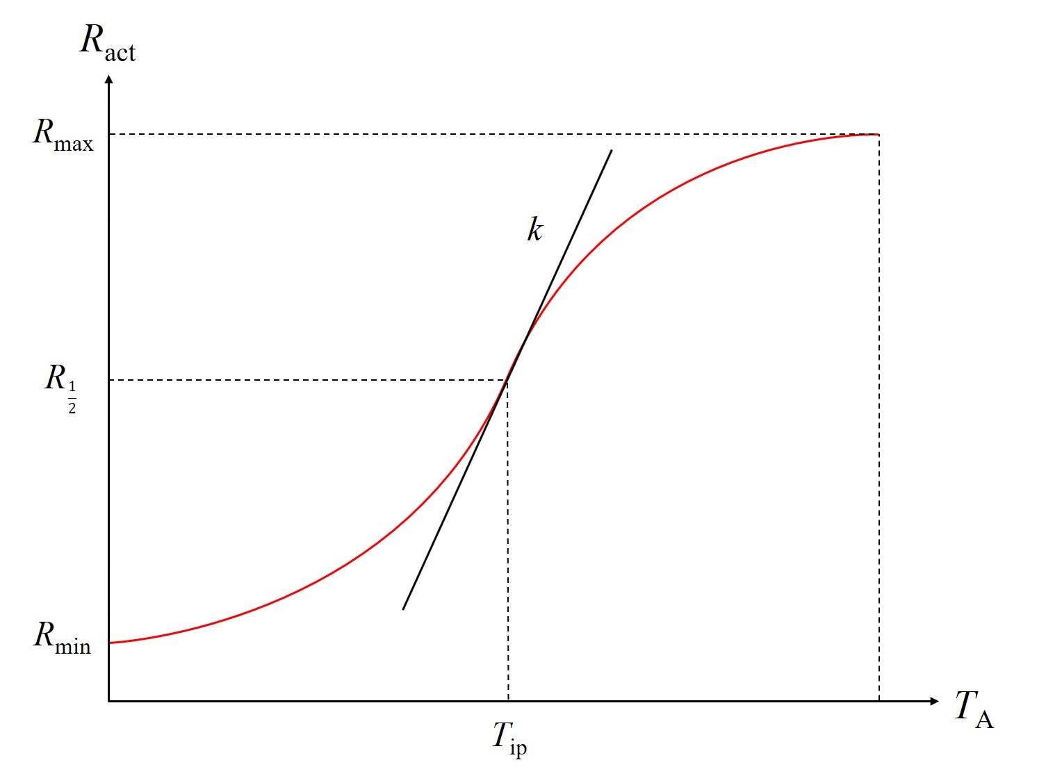
\begin{equation} R_\mathrm {act} = R_{\frac {1}{2}} + \left ( R_\mathrm {max} - R_{\frac {1}{2}} \right ) \tanh \left (k_\mathrm {slope} \ (T_\mathrm {A} - T_\mathrm {ip})\right ), \label {eq:activation_model} \end{equation}
with
\( \seteqsection {3} \) \( \seteqnumber {27} \)
\begin{equation} R_{\frac {1}{2}} = \Big ( \frac {R_\mathrm {min} + R_\mathrm {max}}{2} \Big ). \end{equation}
k, Rmin, Rmax, and Tip are the model parameters. R1/2, Rmax, and Rmin are the half-maximal, maximal, and minimal electrical activation ratio, respectively, kslope is the slope of the step, and Tip the temperature at the inflection of the curve, as shown in Figure 3.5.
3.2.2 Calibration
For the corresponding annealing temperature the donor and acceptor concentrations (obtained via charge neutrality fitting) are incorporated into the ratios of electrical activation via (3.24) and (3.25), respectively. The activation ratios as a function of the annealing temperature for n- and p-type SiC are shown in Figures 3.6 and 3.7. The acceptor and donor concentrations obtained via the charge neutrality fitting are in good agreement with experimental data [1, 151, 152, 130, 153] and provide additional insights into the activation mechanism. The activation ratios are highly temperature-dependent and can be characterized with the activation ratio model accurately predicting the temperature-related effects of the annealing steps. The parameters of the activation ratio model fitting from Figures 3.6 and 3.7 are summarized in Table 3.3.
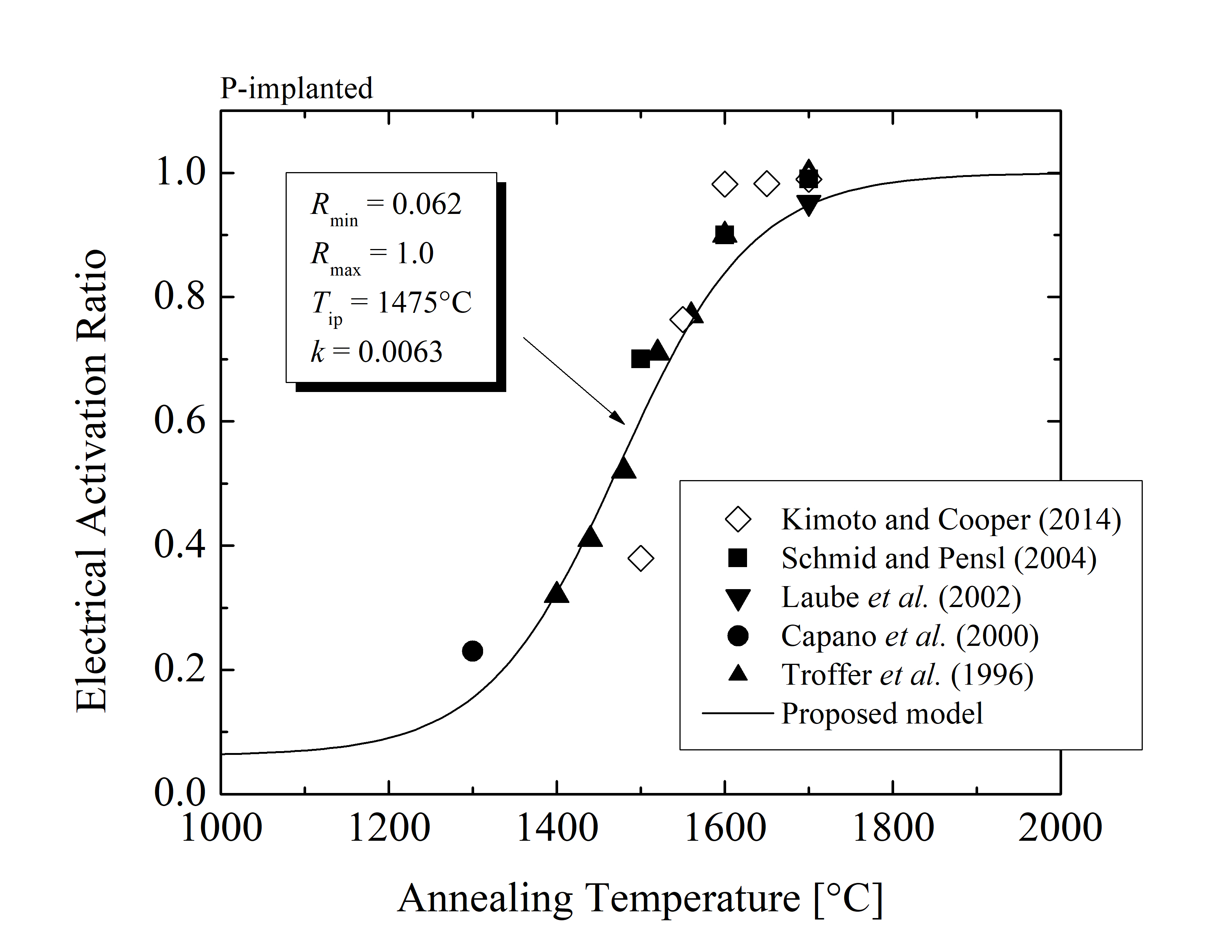
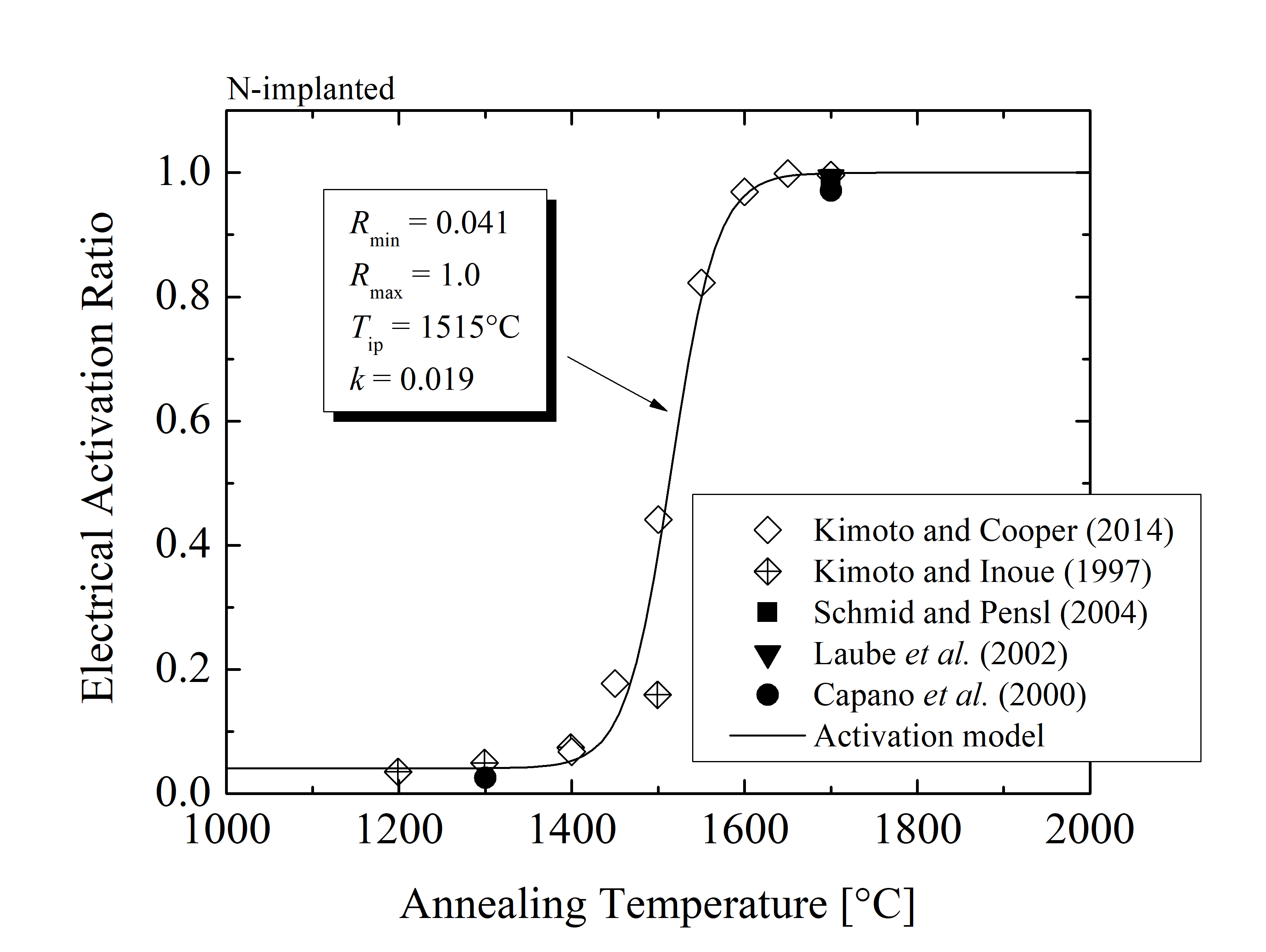
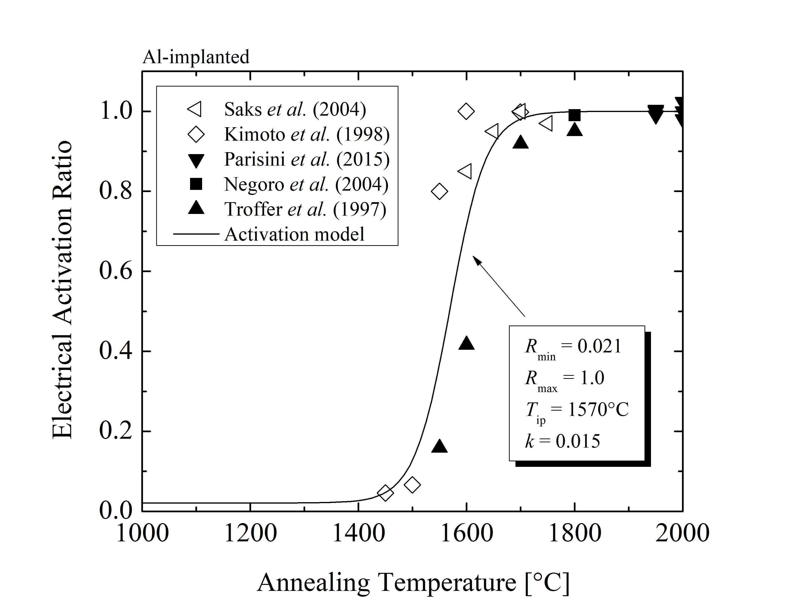
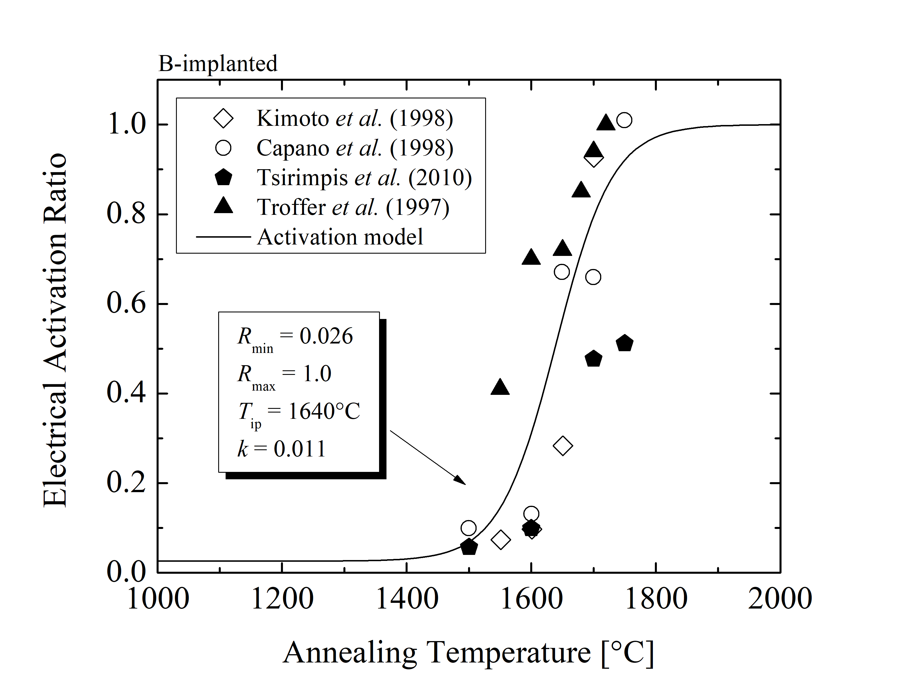
Table 3.3: Model parameters for P-, N-, Al-, and B-implanted SiC.
| Dopant | Rmin [/] | Rmax [/] | Tip [°C] | k [1/°C] |
| P | 0.062 | 1.0 | 1475 | 0.0063 |
| N | 0.041 | 1.0 | 1515 | 0.019 |
| Al | 0.021 | 1.0 | 1570 | 0.015 |
| B | 0.026 | 1.0 | 1640 | 0.011 |
The activation ratio model suggest that the P and N species reach full activation at high temperatures TA > 1700°C and that the minimal activation of both donor-type dopants is approximately 5%. Additionally, the model shows that the ratio of the N-implanted SiC is similar to a step function, while the ratio for the P-implanted SiC increases continuously with temperature, i.e., k(N) ≈ 3k(P). A high activation (above 95 %) is achieved for TA > 1800°C for Al and TA > 1700°C for B impurities and a very low activation (below 10 %) is detected for TA > 1500°C for both Al and B implantations. These findings imply that the thermal activation mechanism dominates within the temperature range 1500°C < TA < 1800°C and must be therefore appropriately characterized, i.e., calculated with the introduced model.
The activation ratio model includes only a dependence on the annealing temperature. For a majority of semiconductor materials the total doping concentration has, in addition to the annealing temperature, a considerable effect on the electrical activation of impurities. For this reason a semi-empirical model is introduced in order to further increase the accuracy of process simulations.