4.2 Design of TSVs
Through Silicon Vias are large structures in comparison to the components inside the
device. The TSVs radius can span from 5 m up to 300
 m and the height usually follows
aspect ratios from 1:1 up to 1:10 in relation to the radius [29][78]. Therefore, if CMOS 90nm
technology is considered, a TSV would solely occupy the area of, at least, several
thousands of transistors. Such a large metal structure in the middle of the device
generates considerable stress, which can lead to device malfunction and cracks in the
silicon.
m and the height usually follows
aspect ratios from 1:1 up to 1:10 in relation to the radius [29][78]. Therefore, if CMOS 90nm
technology is considered, a TSV would solely occupy the area of, at least, several
thousands of transistors. Such a large metal structure in the middle of the device
generates considerable stress, which can lead to device malfunction and cracks in the
silicon.
Thermal and residual stresses account for several reliability issues in TSVs. Consequently,
they have become a major concern in mechanical stability designs [79][80][81]. The
thermo-mechanical stress arises from the difference between the coefficient of thermal
expansion (CTE) of silicon – which surrounds the via – and the interconnection metal.
Meanwhile, the residual stress results from different physical mechanisms which take place
during metal deposition.
The impact of each stress component can be controlled by the choice of materials and the
geometry forming the TSV. A good design should manage the mechanical issues while not
compromising the electrical properties of the device. One of the most common and well
documented layouts is the cylindrical copper TSV. The good electrical properties of copper
and the ease of fabrication are an advantage of this technology. However, the difference of
more than one order of magnitude between silicon CTE and copper CTE compromises its
mechanical reliability.
CTE mismatch can be compensated with various strategies, for instance by the use of
polymer liners around the TSV [82]. The liners work as a barrier which absorbs the stress
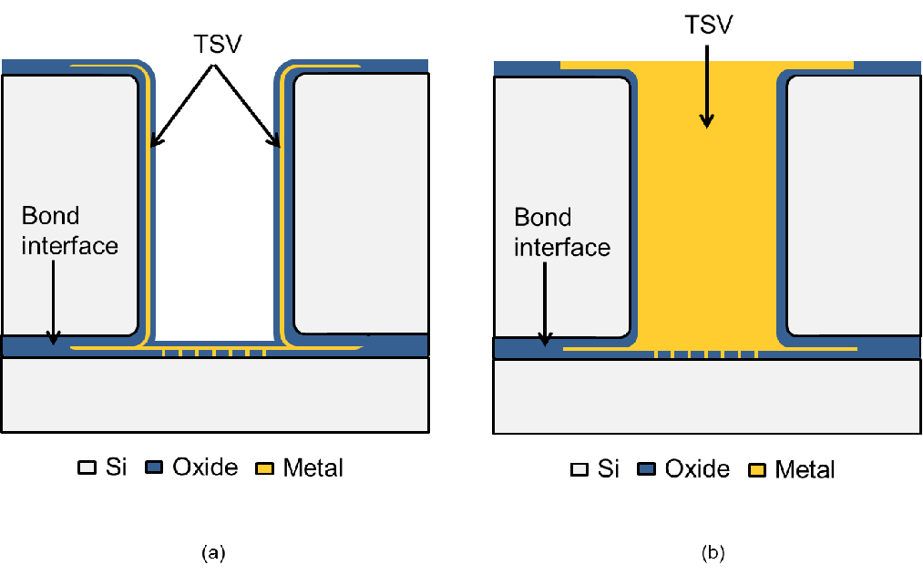
and hinder its propagation towards the silicon. Another approach is the use of an open
(unfilled) TSV instead of a filled via [82][83]. This scheme reduces the amount
of material in the structure and provides room for the metal to expand freely
towards the axis of the via, leading to an overall stress reduction (depending on
the metal properties as will be discussed in the next section). Additionally, the
stress induced by the TSVs in the silicon can be attenuated by their particular
placement [83]. A device usually has several vias close to each other, which can be
arranged in such a way that the stress is mutually cancelled or reduced between
them.
Circular shaped TSVs are preferred over other polygonal geometries. Such designs results in
stress accumulation points in the corners without bringing any particular advantage to the
overall process complexity or device performance.
This work attempts to cover two of the most frequent types of TSVs, filled TSVs and
unfilled (open) TSVs. However, special attention is given to the open TSVs due to a
lack of documentation and available information in the literature. Although the
TSVs can generally be classified in two types, each TSV technology has minor
modifications to handle local stress problems or even to treat processing challenges
such as layer delamination, material diffusion or to improve layer adhesion. In
order to establish a common ground for discussion, during this work two standard
TSVs are considered, as shown in Fig. 4.1: one for filled vias and another for
unfilled vias. Any deviation from the standard discussion of TSV performance and
reliability will be properly addressed and explained in the text. The design is
based on a previous TSV technology [8][29], for which experimental data were
available.
 m diameter and 250
 m height. Filled
TSVs are usually smaller than the one presented here, however, the dimensions were
chosen in order to allow for a fair comparison between both technologies.
m height. Filled
TSVs are usually smaller than the one presented here, however, the dimensions were
chosen in order to allow for a fair comparison between both technologies.