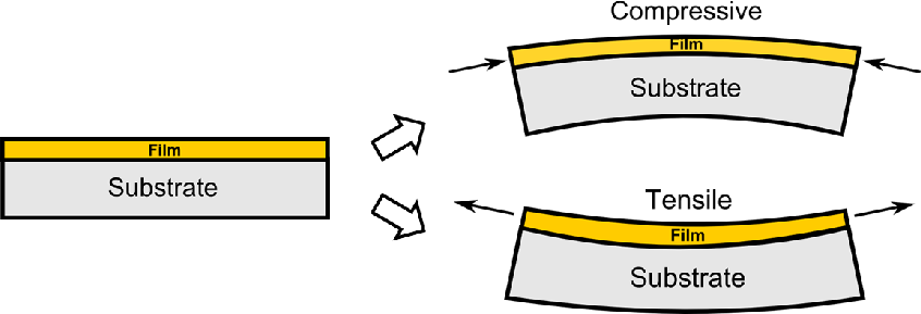
| Figure 5.12.: | Wafer bow due to film deposition. The curvature depends if the film stress is tensile (positive) or compressive (negative). |
This section mainly deals with a different scenario, although the context of device processing and its influence on TSV performance is still present. The central purpose of this section is to understand how the handling of the wafer on a macroscale (millimeters) can affect the stress in the TSV. For that examination one should understand the conditions in which a wafer is found after TSV fabrication, more specifically after thin film deposition.
Film depositions usually modify the wafer shape. They are generally performed at several degrees above room temperature. At deposition temperature the material conforms to the substrate and an intrinsic stress arises as result of several processes during film formation, as described in Table 5.1.
After deposition the wafer is cooled down, but the film and the substrate contract at
different speeds, due to the difference in the coefficient of thermal expansion (CTE
mismatch). The variation of temperature creates stress in the materials, which increases the
intrinsic stress. In order to accommodate these additional stress effects and reach a stable
state, the system will bow itself up or down, depending on whether the resultant stress is
positive or negative as shown in Fig. 5.12.
| Figure 5.12.: | Wafer bow due to film deposition. The curvature depends if the film stress is tensile (positive) or compressive (negative). |
G.G. Stoney in 1909 developed an elegant method to determine, from the wafer curvature, the stress state of the film as in [89]
 | (5.2) |
where  is the average stress on the plane of the film,
  is the biaxial elastic modulus
of the substrate,
is the biaxial elastic modulus
of the substrate,  is the substrate thickness,
  is the film thickness, and
  is the
system curvature.
is the
system curvature.
At the time Stoney made strict constraints which were removed, as film deposition studies progressed by several works which included more sophisticated systems and multiple layered films [89]. This work does not intend to extensively discuss such models, but instead to provide a brief explanation for wafer bowing.