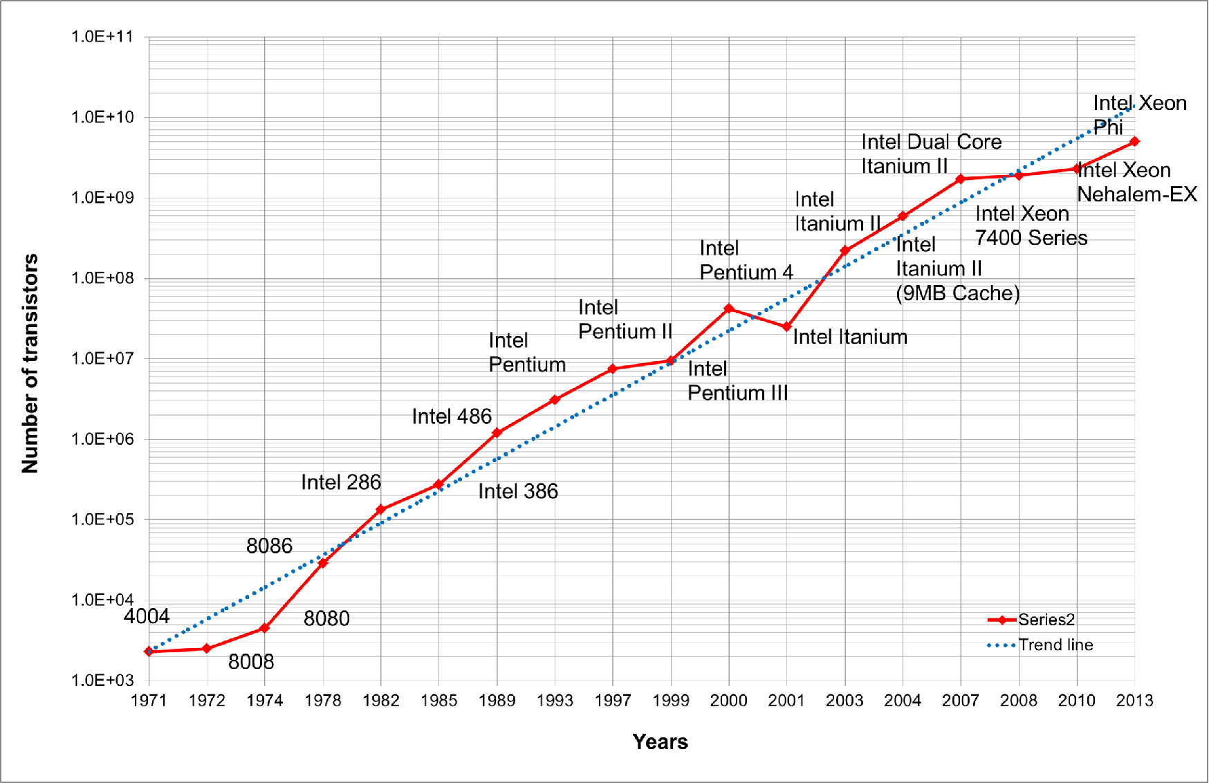
| Figure 1.4.: | Moore’s law in semi-log scale. |
After the successful invention of the IC, the benefits of continuous integration became evident as time progressed. Smaller devices yielded higher speed, lower power consumption, and reduced manufacturing costs, since it was possible to produce more devices on a single wafer [13]. Gordon Moore, a renowned pioneer in the semiconductor industry, predicted in 1965 that the number of transistors on IC would double approximately every two years, a trend shown in Fig. 1.4 [13][14]. His estimative has been proven accurate through the years, but such exponential growth cannot persist indefinitely. A minor slow-down in the miniaturization pace has already been detected and leading foundries have been discussing the post-Moore era [15][16][17].
Further integration in the current semiconductor technology is bounded by device operation and processing limitations. A not exhaustive list is presented below with the most common scaling problems for various applications.
When analyzing digital circuits, a transistor has two modes of operation: “on” and “off”. Ideally, the current flows through the device only, when the transistor is “on”. During the “off” state the flow is blocked and there is no power consumption. In real devices the “off” state is not completely free of power consumption. There is a small current flow, which should be negligible in comparison to the “on” state. Such undesired flow of current in a transistor is defined as current leakage [18].
As the devices get smaller current leakage increases mainly by two mechanisms. The first is known as gate leakage. It occurs due to the thin gate isolation in smaller devices. In that situation the electrons present in the gate tunnels to the conducting channel, deteriorating the transistor operation. The second mechanism is the subthreshold leakage. The channel length and threshold voltage of a transistor decreases as the overall device size decreases. The reduction of these two parameters increases the current flow between drain and source during “off” state. Leakage currents are severe problems of modern devices fabrication and, in some cases, they can account for more than 50% of the device’s power consumption [19].
Smaller devices are very susceptible to eventual processing deviations. For example, as described by Haselman and Hauck [18], the gate oxide in current devices is only five atoms thick. A misplacement of only one atom can modify the device design specification by 20%. Such sensitivity of device fabrication can damage yield and increases fabrication costs.
For many years, lithography improvements were made by enhancements on the lens, improvements in the imaging material technology, and the reduction of the source wavelength. Naturally, it is expected that at some point the feature size becomes smaller than the resolution power of optical systems [18][20]. In fact, such a situation is already true in modern lithography technology. The 32nm node had to implement advanced optical techniques such as, optical proximity, phase-shift masks, and immersion lithography [21]. However, those enhancements are not enough for the 22nm and 16nm nodes, and new advancements in pattern transfer are needed [20][21] [22][23].
The increasing integration of devices demands longer and thinner interconnects. Such conditions lead to slower interconnections and higher power dissipation, increasing the device temperature during operation. Low resistivity metals and low-k oxides are currently employed to ease the Joule dissipation and signal delay, respectively [24]. However, they suffer from processing and reliability problems which can lead to increased production costs. The interconnection can be engineered in a more efficient way with the development of optical interconnects and three-dimensional (3D) integration technologies.