6.1 Growth of Metal Films
Metal films can be deposited using several methods which can be separated in two
general groups: chemical vapor deposition (CVD) and physical vapor deposition
(PVD) [38][95]. The former comprises the entire range of techniques which use
volatile compounds to deliver the metal atoms to the substrate. The different
types of CVD depositions are usually distinguished by a particular characteristic
of the deposition condition (e.g. low pressure, aerosol assisted deposition, metal
organic compounds as precursors, etc.) [95]. In the semiconductor industry, plasma
enhanced CVD (PECVD) is widely employed. During PECVD processing, plasma
discharges are applied to the film-substrate system during deposition. The high
energetic electrons from the plasma enable reactions which would otherwise not be
possible at low temperatures. Such features are very important during BEOL,
where temperature variations are limited. Furthermore, PECVD is known for
increased film adhesion, high deposition rates, and lower resulting deposited film
roughness.
PVD includes any technique which utilizes a physical mechanism to transport the metal to
the substrate [38]. For example, sputtering is a very popular PVD method in the
semiconductor industry. It consists of the ejection of metal atoms from a material source
(thin slab) by an inert gas (usually Ar). The atoms of the gas are ionized and accelerated
toward the source, the impact causes the release of some metal atoms which travel to the
substrate, where they are deposited. The different types of PVD are sorted accordingly to
the physical mechanism implemented to release source atoms. In addition to sputtering,
evaporation, and electron beam PVD are frequently employed during semiconductor
fabrication.
Each deposition method has its advantages and disadvantages. CVD generally has a better
step coverage and film quality, but one must deal with hazardous products contained in the
chemical reactions. On the other hand, PVD is available for a wider variety of materials (no
volatile compound needed) and is more environmental friendly. Ultimately, the deposition
method is chosen based on the desired application and eventually financial constraints
[66][95][96].
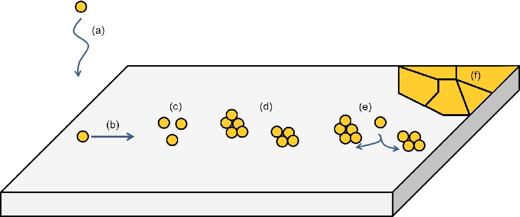
Regardless of the applied deposition technique, thin film growth is a process with at least six
fundamental steps [38]:
- The material is transported to the substrate, where physical interaction takes
place and the deposited atoms become weakly attached to the surface.
- The adatoms – it is common in the literature to refer to atoms which lie in a
crystal surface as adatoms – diffuse over the substrate towards low energy sites.
Depending on the affinity of the adatoms and the substrate, a chemical bond is
formed between them.
- At this point a cluster of adatoms merges at several locations in order to minimize
the system energy, a process known as nucleation.
- As these agglomerates grow bigger and approach each other, film coalescence
occurs. This process takes place, when two or more droplets come in contact
during growing and merge to form a continuous material.
- The islands compete against each other for the arriving adatoms, until the entire
substrate is covered. The remaining droplets delineate the grain boundaries,
forming the film microstructure.
- Finally, film deposition ceases and processes, such as grain growth and diffusion,
take place, depending on the environmental conditions. The entire process is
summarized in Fig. 6.1.
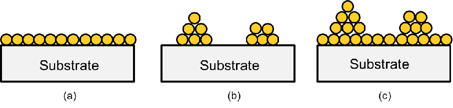
Depending on a material’s affinity and environmental conditions, the growth process
described above can be carried out in one of three different modes known as Frank-van der
Merwe (FM), Volmer-Weber (VW), and Stransky-Krastanov (SK) growth[97]. In FM mode
the adatoms are very compatible with the substrate and prefer to attach directly
on it, hindering the formation of clusters. Therefore, the film coverage is very
smooth and conformal to the substrate. In VW mode the opposite is the case. The
interaction between the adatoms of the deposited material is stronger than the
interactions of the adatoms and the surface. Consequently, more islands of the deposited
material are formed. The SK mode is a mix of FM and VW. In this mode the growth
follows the FM pattern, until the film reaches a critical thickness. When this critical
thickness is reached, VM mode takes over and the islands are created as depicted in
Fig. 6.2.
Metals deposited on a surface of silicon dioxide usually form thin films using the
Volmer-Weber growth mode [98][99]. In this chapter this will be the only mode considered,
since the entire discussion revolves around the residual stress in metal layers of TSVs. For
the considered TSV, the metal layer is deposited on a silicon dioxide layer, meaning that the
Wolmer-Weber growth model is expected.