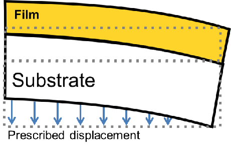
m negatively is forced flat by an external force, as depicted
in Fig. 5.13.
m negatively is forced flat by an external force, as depicted
in Fig. 5.13. A curved wafer is a common occurrence during semiconductor processing and TSVs are
susceptible to its effects, especially in cases which disturb the bowed stable state. For
instance, during handling the wafer can be forced to a flat state with a machine chuck for
further processing or transportation. In such scenarios a question immediately arises: would
a flattening process cause mechanical instability in the TSVs? In order to find an answer,
imagine that a wafer bowed 3m negatively is forced flat by an external force, as depicted
in Fig. 5.13.
To assess the impact of the flattening process, mechanical FEM simulations were performed.
The simulation setup in this case is more challenging, because of the scale difference
between the considered structures. A wafer has a diameter of up to 300mm while a standard
TSV radius measures in the range of 100 m. The difference in length scales creates several
complications for the simulation regarding meshing, numerical stability, and computing
time.
m. The difference in length scales creates several
complications for the simulation regarding meshing, numerical stability, and computing
time.
A different approach is required in order to create a manageable simulation environment.
The problem was treated in a hierarchical manner, where the simulation starts with a
domain in a length scale comparable to the wafer diameter and is reduced, until the length
scale of only one TSV is reached. A schematic of the adopted strategy is depicted in
Fig. 5.14.
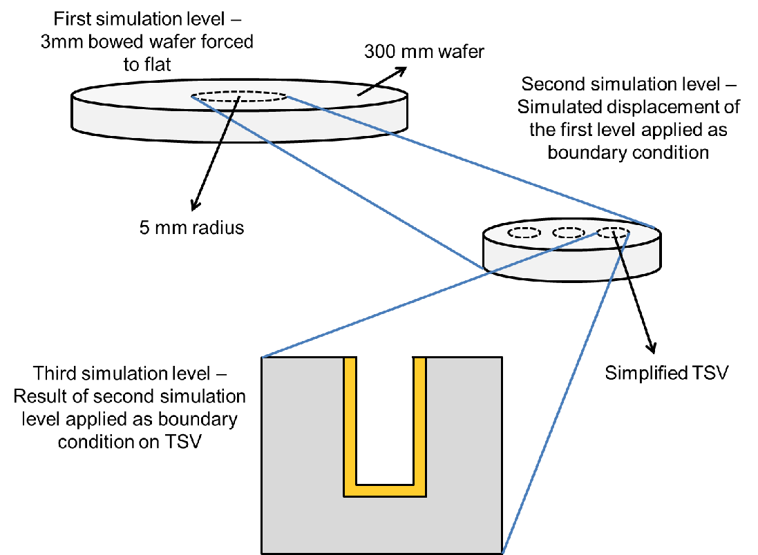
| Figure 5.14.: | Schematic of the multilevel approach for a simulation of large scale effects in the TSV. |
At each step simulation level a simulation is required and the result is passed as a boundary condition to the next level. For example, the simulation starts with the flattening process of the entire wafer. At this point no TSVs are present in the domain, only the wafer is considered. In the next step the domain is reduced to a radius of 5mm from the wafer center. The TSVs are already present in a simplified manner, they are represented with holes in the silicon without any additional thin material layers. The computed displacement of the previous step is then applied as a boundary condition, forcing the solution to match at the domains’ intersection. Finally, the domain reduction process is applied again to a single TSV. All material layers are present in this last simulation, where the boundary conditions are again computed using the displacement calculated at the previous simulation level.
This multilevel approach allows for the treatment of features on domains with very different scales. The complexity of the structures are included gradually, which reduces the computational cost of including all features at all simulation domains. The weakness of this technique lies in the boundary conditions of the lower levels, since their quality is limited by the solution of the upper levels. Therefore, a better refinement of the mesh of the domains in the respective lower levels is needed to obtain reliable results. Additionally, domain reductions of several orders of magnitude create numerical instability, because the mesh might not be fine enough to resolve very small domains. For example, a reduction from the wafer level directly to the TSV level would be a problem, since it would be necessary for a mesh element located in the region of a TSV to resolve the detailed TSV region, increasing drastically the computational requirements. The multilevel simulation strategy described here can also be seen as a special case of domain decomposition methods [90].
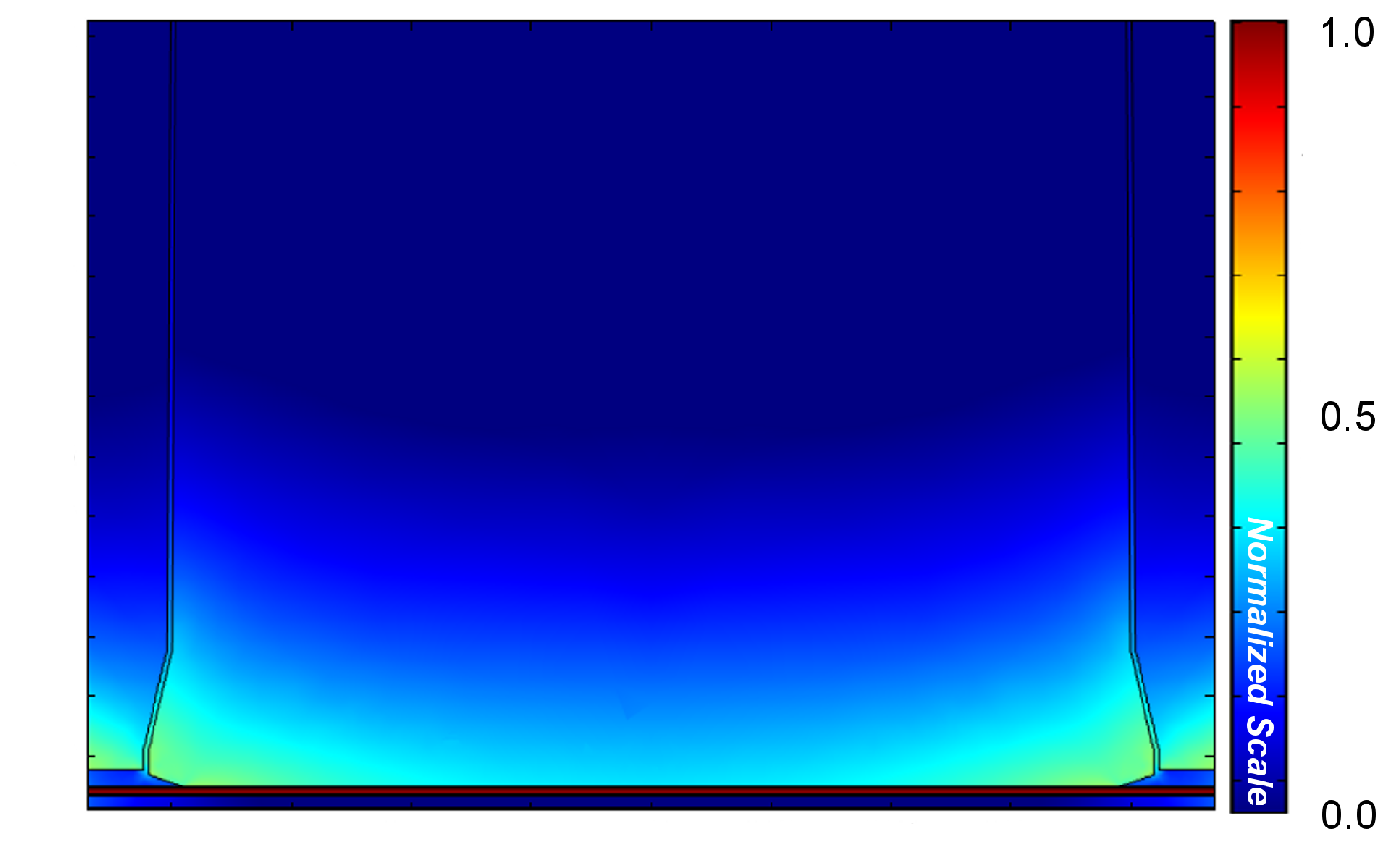
The result of the simulation for the last level of the filled TSV is depicted in Fig. 5.15, while
the results from all simulation levels for an unfilled TSV are shown in Fig. 5.16. Measured
intrinsic stress is considered on the film layers at the TSV level (last simulation). The stress
at the TSV bottom of the unfilled via is very high, especially at the corners. The structure
at this region acts like a lever and the stress generated by the “unbow” motion is magnified,
producing potential failure spots on the TSV. Filled TSVs are better supported
in this situation. The metal inside the cavity hinders the lever-like movement,
increasing the mechanical stability of the structure against wafer handling situations.
| Figure 5.15.: | Result of the last simulation level of a multilevel simulation of a filled TSV. The material inside the cavity provides better support against forces at the bottom of the TSV. |
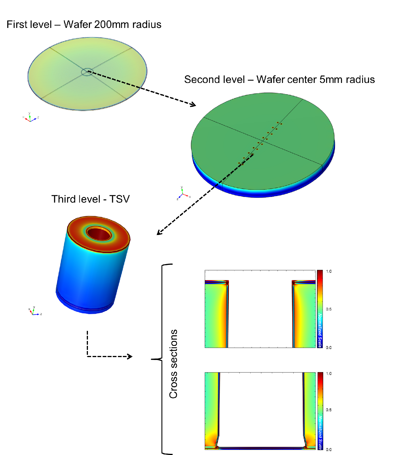
| Figure 5.16.: | Simulation of the effects of a forced unbow on the TSV. In the first level, no TSV is considered. For the second level the vias are treated as regular holes in the silicon. Only at the last level the TSV is considered in full detail. The unbow movement is particularly dangerous for the bottom and top corners of the via. |