Next: 4.2.3 Impact of Pre-stressed Interface State Density Profile on HCD Modeling Up: 4.2 Interface State Profile of Unstressed Device Previous: 4.2.1 Verification of the Interface State Density Distribution Uniformity
Applying this separation technique it is possible to use the technique for Nit extraction developed in [176]. The interface trap concentration of a pre-stressed device can be written as
while using the uniform approach [175] results in
(a)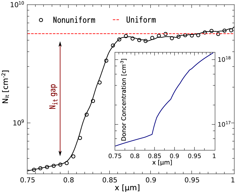 (b)
(b)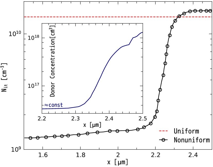
|
Figure 4.7a depicts a comparison between the uniform and nonuniform interface state density profiles. It is believed that the gap in the center of the device can be linked to the peculiarities of the device fabrication process. The inset in Figure 4.7a represents the donor doping concentration with increased gradient at 0.85um where Nit(x) reaches a uniform value, i.e. the transistor doping can affect the interface state density in this way. An identical tendency shown in Figure 4.7b, i.e the correlation between the Nit gap and the donor doping concentration profile, was revealed for the device of the same topology (produced using the same technology) but with a gate length of 2um. Moreover, the non-uniformity of the initial Nit profile can be easily visualized within a constant amplitude CP technique. In this case the gate pulse covers the device interface step by step. According to (4.3), the charge pumping current is proportional to the interface state density averaged over the effective measurement length. Icp,max depicted in Figure 4.8a inset is reached at a base level of -2V. At the same time, the maximal effective length corresponds to -1V, i.e. in this area the Nit concentration is lower. This approach which is based on another measurement setup additionally confirms previous findings.
(a)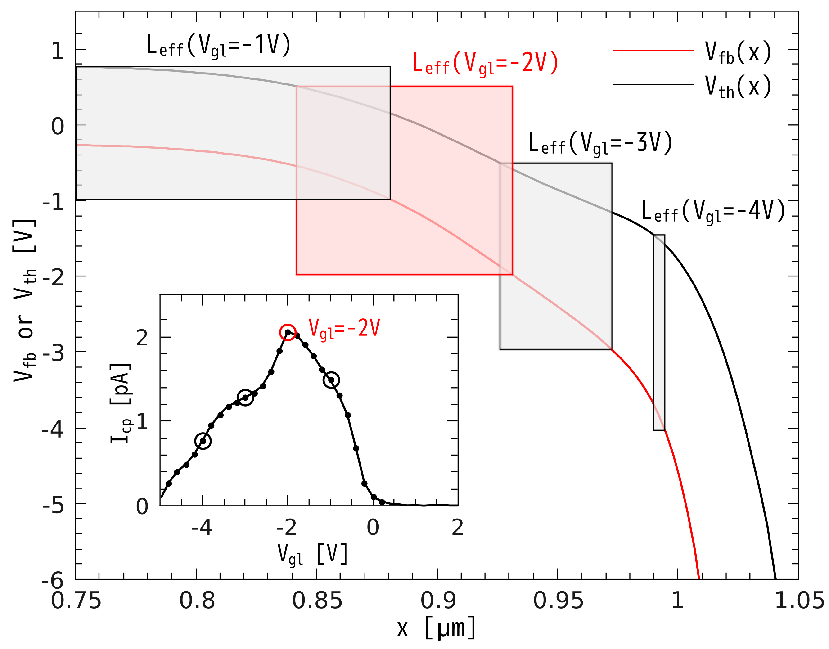 (b)
(b)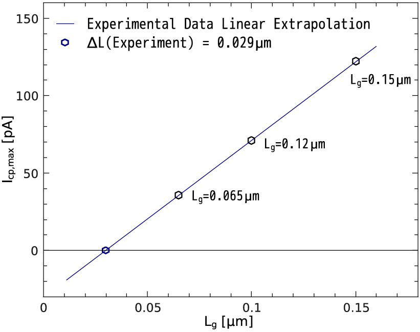
|
However, the demonstrated non-uniformity of the unstressed Nit profile is not a mandatory phenomenon. As an example, a CMOS device fabricated on 300mm (100) Si wafers using a metal-inserted poly-Si process (the high-k dielectric is mainly HfO2) demonstrates in Figure 4.8b a linear dependence between the maximum value of the charge pumping current and gate electrode lengths. This ideal linear graph confirms a uniform initial Nit distribution for such a class of MOSFETs.