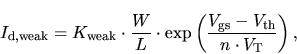
The drain current of a MOS transistor depends on its gate length in several ways. Considering a first-order approximation the current is inversely proportional to the gate length. Second-order effects include velocity saturation, DIBL, and channel length modulation [65].
For drive current optimizations with a constant leakage current the reduction
of the effective gate length is one possible choice. This becomes obvious
when the drain-current expressions for weak and strong inversion are taken
into account. In a first order approximation, the drain current depends
exponentially on the threshold voltage for weak inversion
When the gate length is reduced, both the leakage and drive currents will rise. Therefore, the threshold voltage has to be increased to keep the leakage current unchanged and the drive current will rise because of its smaller threshold voltage dependence. However, there is a lower limit for the gate length where no further drive current improvements can be achieved because threshold voltage reduction due to DIBL becomes significant. If the gate length falls below this limit, the necessary increase in the bulk doping to account for the reduced threshold voltage will lead to a poor subthreshold slope due to the increased bulk effect.
Fig. 5.3 shows the drive current versus gate length of a uniformly doped device with 5 nm oxide thickness and 1 pA leakage current for 1.5 V supply voltage. Data were extracted in three ways: (a) using two-dimensional device simulations with MINIMOS-NT, (b) the analytical drain-current model including DIBL, and (c) the same model without DIBL. Threshold voltage adjustment was done by bulk doping variation to keep the leakage current constant. The drain-current model includes the following second-order effects: DIBL (optionally), velocity saturation, and mobility reduction due to impurity scattering. Appendix C gives a detailed description of this analytical model.
![\resizebox{0.95\textwidth }{!}{
\psfrag{xlabel} [ct][ct] {gate length {
{$L_{\ma...
...ct] {1}
\includegraphics[width=0.95\textwidth ]{../figures/peaklength-pcd.eps}}](img140.gif)
|
It can be seen that for a uniformly doped device there exists an optimal gate length where the drive current reaches a maximum. For 1.5 V supply voltage this optimum is about 80 nm. The above results can be used to give an explanation for the superior drive performance of the PCD device: The effective transistor is restricted to a short region near the source. The rest of the channel region works like a depletion-type cascode transistor which only sets the drain voltage of the effective transistor and does not influence its performance in the saturated case. Therefore, the advantages of a short transistor, as discussed above, also apply for the PCD device, even if the overall gate length of this device is high.
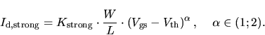
Fig. 5.4 shows the optimal gate length of the same uniformly doped device for various gate and drain voltages, derived by the analytical drain-current model with DIBL. If the drain voltage is increased while the gate voltage is fixed at 1.5 V, as shown in curve (a), the optimal gate length becomes larger to reduce the DIBL effect.
Two-dimensional device simulation have shown that the voltage at the right-hand side of the doping peak in the PCD device is about 0.5 V. With the drain voltage fixed at this value, as shown in curve (b), the optimal gate length becomes very large if the gate voltage falls below the anticipated threshold voltage of the device. The optimal gate length decreases if the gate voltage becomes higher. The drive current enhancement due to the different current-voltage relationships (5.1) and (5.2) can be exploited only if the device is operated in the strong inversion regime during the on-state. This effect is stronger in the strong inversion regime.
If the gate and the drain voltages are varied coincidentally, which is the most common case, the two effects superpose, as shown in curve (c), with a minimum of the optimal gate length at about 1.5 V.
![\resizebox{0.95\textwidth }{!}{
\psfrag{xlabel} [ct][ct] {gate voltage {
{$V_{\m...
... {5}
\includegraphics[width=0.95\textwidth ]{../figures/optgatelength-pcd.eps}}](img141.gif)
|