« PreviousUpNext »Contents
Previous: 1 Introduction Top: 1 Introduction Next: 1.3 Goal of this thesis
1.2 Defects in GaN/AlGaN MIS–HEMTs
The first GaN–based devices are nowadays available on the market, however there is still a number of issues to be investigated in order to achieve a comprehensive understanding of all their failure mechanisms. In particular, reliability is a major concern, as charge trapping phenomena result in severe drift effects.
In the following, we introduce the most important reliability issues for GaN–based HEMT and MIS–HEMT structures, and then we focus on the two main areas where defects play a role for the device degradation: bulk defects and interface states, giving an overview of the state–of–the–art.
1.2.1 Reliability issues of GaN–based devices
The main problem of GaN–based devices today is to guarantee high–performance during operation together with a high level of stability, especially in their dynamic response. The primary cause is to be found in charge trapping phenomena.
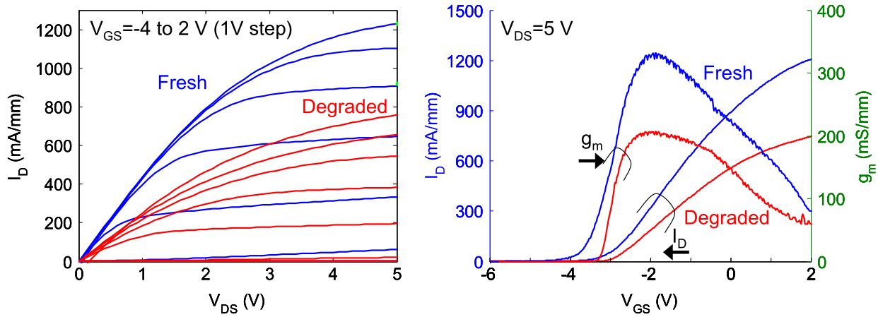
One of the major issues is the current collapse effect, i.e., the recoverable decrease of the drain current during operation, after a gate or drain voltage change [16, 17]. An example is shown in Fig. 1.6a. This phenomenon is studied by performing single– or double–pulsed drain current measurements, during which the drain current is monitored in on state after the application of a stress transient, usually in off state [18, 19]. The analysis of the time evolution of the drain current during recovery allows to extract some properties of the defects responsible for charge trapping.


Trapping of 2DEG electrons can take place at different locations within the device structure. One possibility is at or below the gate stack, which means charge injection in the substrate, or trapping in the AlGaN layer or the GaN buffer. Even though the material quality has been constantly improving over the years, the main source of defects is still the GaN substrate, namely the deeper GaN layers. The reason is the need for a progressive change in lattice constant because of the non–native substrate (in our case, silicon), which leads to dislocations in the bulk material, or the use of dopants which may act like charge trapping sites as well. This results in as a negative drift of the threshold voltage after stress in off state (at negative gate biases), which causes the whole transfer characteristic to shift towards more negative values of gate bias [20].
Another effect related to the current collapse is the degradation of the dynamic on–resistance, also visible as  transconductance reduction (Fig. 1.6b). This can be due to charge trapping at the surface in the access region [21], because of defects at the surface or close to the passivation layer [22]. Another phenomenon responsible for
the reduction of on–resistance is hot electron degradation. This happens when the drain voltage is high and very large electric fields are present. Hot electrons can generate traps in the access region, thus damaging the material structure and leading to the
degradation of the electron mobility [17]. Since the on–resistance is the most critical parameter for switching applications, further investigations aimed to understand and reduce this problem are of primary importance [23].
transconductance reduction (Fig. 1.6b). This can be due to charge trapping at the surface in the access region [21], because of defects at the surface or close to the passivation layer [22]. Another phenomenon responsible for
the reduction of on–resistance is hot electron degradation. This happens when the drain voltage is high and very large electric fields are present. Hot electrons can generate traps in the access region, thus damaging the material structure and leading to the
degradation of the electron mobility [17]. Since the on–resistance is the most critical parameter for switching applications, further investigations aimed to understand and reduce this problem are of primary importance [23].
A further source of degradation can be due to the piezoelectric qualities of GaN and AlGaN. If a large electric field is applied, the material would experience a certain amount of stress. This may eventually lead to the formation of electrically active crystallographic defects [16].
Finally, device breakdown can occur as a consequence of defect generation under large electric fields. If the density of defects rises so much to form a percolation path, conduction takes place primarily along this conductive way. This leads to catastrophic gate leakage current in the case of vertical breakdown of a GaN HEMT, or to current flowing out of the source terminal if the percolation path is formed between drain and source [23]. Investigations over a large number of Schottky devices show that the time dependence of gate breakdown follows a Weibull distribution [24].
1.2.2 Activation energy and thermodynamic energy level of defects
At this point, it is necessary to introduce some physical concepts about charge exchange mechanisms, and to define the activation energy of a defect for trapping and detrapping events. Depending on the model and the degree of simplification used, the activation energy can be defined in different ways. Unfortunately, this might lead to a misinterpretation of its physical meaning. For this reason, we present here briefly the non–radiative, multiphonon model for charge exchange, in contrast to the Shockley–Read–Hall (SRH) theory. Both models are discussed in more detail in Chapter 4.
The trapping (or detrapping) of an electron (or hole) results in the change of the charge state of a defect site present in the device under test. The transition between two charge states corresponds to a transition between two different configurations of the
defect. Each configuration is defined by a certain equilibrium position of the atoms constituting the defect, which is given by the result of all the quantum–mechanical repulsive and attractive forces. Furthermore, in the Born–Oppenheimer approximation the
atoms vibrate around their equilibrium positions depending on the temperature. We can therefore describe each status of the system, for example an empty and a filled trap level, as harmonic oscillators along a certain reaction coordinate  , as shown in Fig. 1.7 [25]. The equilibrium energy and the coordinate of the two configurations of the defect are different: in fact,
the spatial arrangement of the atoms constituting the trap site changes according to its charge state, since the bonds to the captured or emitted electron must be created or destroyed. The difference between the minimum of the two parabolas is called the zero
phonon energy,
, as shown in Fig. 1.7 [25]. The equilibrium energy and the coordinate of the two configurations of the defect are different: in fact,
the spatial arrangement of the atoms constituting the trap site changes according to its charge state, since the bonds to the captured or emitted electron must be created or destroyed. The difference between the minimum of the two parabolas is called the zero
phonon energy,  . However, in order to make the transition possible, some
excess energy must be supplied to the system. The absorption of optical energy results in vertical transitions in the diagram of Fig. 1.7, according to the Franck–Condon principle [26].
Therefore, an amount of optical energy equal to
. However, in order to make the transition possible, some
excess energy must be supplied to the system. The absorption of optical energy results in vertical transitions in the diagram of Fig. 1.7, according to the Franck–Condon principle [26].
Therefore, an amount of optical energy equal to  is necessary for the transition from state 1
to state 2. The difference with is the relaxation energy
is necessary for the transition from state 1
to state 2. The difference with is the relaxation energy  , also called Franck–Condon shift. It can be
expressed as the product of the Huang–Rhys factor
, also called Franck–Condon shift. It can be
expressed as the product of the Huang–Rhys factor  and the effective phonon energy
  :
:  .
.
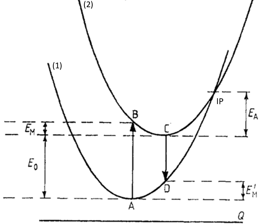
Figure 1.7: Illustration of a two–level system, for example a defect site that can be empty (1) or filled (2). Some possible transitions are indicated: the direct transition from 1 to 2 through optical energy absorption (A to B) and the transition from 2 to 1 with emission of optical energy during photoluminescence (C to D). The non–radiative, multiphonon transition between the two states takes place through the intersection point, IP (adapted from [25]).
Furthermore, the energy  is released
during the transition from 2 to 1 with a photoluminescence experiment. On the other hand, in absence of electromagnetic radiation the transition between the two states is mediated by phonons. For this reason, in a semi–classical approximation a non–radiative
multiphonon (NMP) transition must take place through the intersection point (IP). In this way, the activation energy for the transitions between the two configurations is defined. For example, a transition from state 2 to 1 in Fig. 1.7 requires the activation energy
is released
during the transition from 2 to 1 with a photoluminescence experiment. On the other hand, in absence of electromagnetic radiation the transition between the two states is mediated by phonons. For this reason, in a semi–classical approximation a non–radiative
multiphonon (NMP) transition must take place through the intersection point (IP). In this way, the activation energy for the transitions between the two configurations is defined. For example, a transition from state 2 to 1 in Fig. 1.7 requires the activation energy  to be provided by phonons.
Another important concept is the thermodynamic energy level of a trap state,  , namely its position inside the semiconductor (or
dielectric) bandgap, as shown in Fig. 1.8. In this way we can determine the position of the defect relative to the Fermi level,
, namely its position inside the semiconductor (or
dielectric) bandgap, as shown in Fig. 1.8. In this way we can determine the position of the defect relative to the Fermi level,  . If lays below , then an electron can be trapped (or a hole
emitted). On the contrary, if
. If lays below , then an electron can be trapped (or a hole
emitted). On the contrary, if  an electron can be emitted (or a
hole trapped). However, according to the SRH model the thermodynamic energy defines the activation energy for capture and emission as well. As shown in Fig. 1.8 in the case of
electrons, there is an energy barrier only for emission, given by the difference between and the edge of the conduction band,
an electron can be emitted (or a
hole trapped). However, according to the SRH model the thermodynamic energy defines the activation energy for capture and emission as well. As shown in Fig. 1.8 in the case of
electrons, there is an energy barrier only for emission, given by the difference between and the edge of the conduction band,  .
.
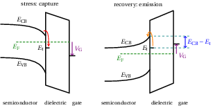

Figure 1.8: Illustration of the thermodynamic energy level of a defect acting as an acceptor trap level, , at the interface between the semiconductor and
the dielectric in a MIS structure during accumulation (a) and depletion (b). According to the SRH model, the energy  alone defines the activation energy
for charge exchange.
alone defines the activation energy
for charge exchange.
In addition to other limitations that are discussed in Chapters 3 and 4, the SRH picture implies that “shallow” states, i.e., defects located close to the conduction band, must have a small activation energy, while “deep” states, located far from , must have a large . On the contrary, experimental evidence has proven the
existence of “shallow” trap states in silicon MOSFETs, responsible for negative bias temperature instability (NBTI), with very large activation energy [27].
In the following sections and in the rest of the thesis, we use the definition of activation energy derived from the NMP theory. In the case of electrical measurements, the activation energy is , the difference between the equilibrium energy of the
initial state and that at the intersection point. On the other hand, the activation energy measured with experimental techniques involving light absorption, like the deep level optical spectroscopy (DLOS), is the optical activation energy  .
.
1.2.3 Bulk defects
The need for a foreign substrate to grow the GaN buffer impacts the material quality, leading to dislocations, vacancies and other lattice irregularities. In addition, impurities like carbon and oxygen are usually found in the GaN bulk, as they are incorporated
during growth [28]. For this reason we talk about unintentionally doped (UID) GaN. In particular, carbon is an amphoteric dopant (i.e., it can act both as a donor or as an acceptor) that can substitute one nitrogen atom ( ) in n–type GaN, or a gallium atom (
 ) in p–type GaN [29, 30].
Some of these defects have been simulated with ab initio calculations, as well as investigated with a number of experimental techniques. Electronic structure and formation energies of the defects can be obtained with quantum molecular dynamics
and the density functional theory approach [29, 31], that allow to draw a picture of the possible configurations when one atom is missing, or the probability for dopants to substitute a Ga or N atom. These values can then be compared with experimental
results. Among the numerous possible experimental techniques we find luminescence investigations [30] or scanning capacitance microscopy, a technique based on contact mode atomic force microscopy (AFM) [28]. However, the most important and widely
used methods are deep level transient spectroscopy (DLTS) [32], and its variation including optical excitation known as deep level optical spectroscopy (DLOS) [33]. While DLTS investigations allow to excite defects with activation energies up to 1 or 1.5 eV,
monochromatic light can access states with activation energies in the order of the semiconductor bandgap (for GaN,  3.39 eV, equivalent to ultraviolet radiation
at 365 nm).
3.39 eV, equivalent to ultraviolet radiation
at 365 nm).
A number of studies have been carried out on bulk materials (GaN and AlGaN with various aluminum content and grown in different ways) and on fully–processed devices. While some defects have been identified, for other observed energy levels the root cause is still unknown, or more than one possible candidate has been suggested.
| Activation energy | Samples | Interpretation(s) |
| 0.25 eV | GaN | N vacancy |
| 0.6 eV | GaN, GaN/AlGaN HEMT | V –O complex, N vacancy, N antisite –O complex, N vacancy, N antisite |
| 0.9 eV | GaN | N interstitial, gallium vacancy |
| 1.28–1.35 eV | GaN | C interstitial |
| 2.3 eV | GaN/AlGaN HEMT | in the gate stack |
| 2.6 eV | GaN | gallium vacancy, V–H or V–2H complex |
| 3.11 eV | AlGaN | gallium vacancy |
| 3.22 eV | GaN, GaN/AlGaN HEMT | Mg substitutional substitutional |
| 3.28–3.3 eV | GaN, GaN/AlGaN HEMT | C substitutional |
| 3.7 eV | GaN/AlGaN HEMT | Mg or C substitutional in AlGaN |
| 3.85–3.93 eV | AlGaN | Mg or C substitutional |
Table 1.2: Summary of some of the most frequently measured defect activation energies with the DLTS and DLOS methods (from [20, 34, 35]).
Several defect levels have been measured in bulk GaN by various authors [20]. We summarize the most important for the present work in Table 1.2. The levels with relatively small
activation energies have been related to defects intrinsic in the material, or caused by common impurities like carbon and oxygen [36, 37]. The 2.6 eV level has been measured by many research groups, which agree in identifying its root cause as a
gallium vacancy, V, or a complex of one V with one or two hydrogen atoms [34]. The
3.22 eV and 3.28 eV defects are typical of the MOCVD and of the MBE growth methods, respectively [35]. The difference here is the dominant acceptor level, which is Mg in MOCVD and C in MBE. Therefore, the two activation energies can be
associated with the respective dopant.
Bulk AlGaN samples show some other typical energy level, like the 3.11 eV cation (gallium in GaN, Al or Ga in AlGaN) vacancy and the 3.9 eV magnesium or carbon substitutional defect [34, 37]. We note that the same type of defect has a different activation energy when it is found in the GaN bulk or in the AlGaN layer [35].
Finally, most of the levels typical of GaN and AlGaN bulk material can be measured in GaN/AlGaN Schottky HEMTs as well. Still, there are some additional defects which arise only in the fully–processed devices. Among them, the 2.3 eV and the 3.7 eV levels should be located somewhere in the gate stack rather than in the access region [34, 35].
1.2.4 Defects at the interface with a dielectric
The use of a dielectric on top of the AlGaN layer effectively prevents gate leakage currents, in comparison with Schottky devices [11]. The new interface between AlGaN and the insulator, however, in most cases is far from perfect, thus giving rise to interface and near interface defects. It is also not clear what the exact impact on the surface donor states is.
The very first challenge in untangling this problem is to characterize the interface states. In the past decades, many methods have been proposed and some of them are nowadays established techniques for the characterization of silicon MOS devices and MOSFETs. The most widely used methods are based on the response of the device to a superposition of small– and large–signal excitation, with an impedance measurement. The density of interface states can be extracted from the capacitance characteristic of the device (the capacitance–voltage, or CV curve) with the Terman method, or from the device conductance as a function of the small–signal frequency with the conductance method [38]. These standard methods can be used as comparison tools, i.e., to evaluate the relative amount of defects within different samples. Nevertheless, since the portion of accessible defects depends on measurement parameters like frequency of the small–signal and temperature [39], care should be taken in comparing defect densities extracted with different techniques and parameters. For the same reason, it is essential to optimize the experimental window. For example, if the probing frequency is too high, states with relatively long characteristic time constant would not be able to respond to the applied AC signal. On the other hand, temperature has the effect of decreasing the time constant of the defects, whose response can therefore be accelerated in order to become measurable within the chosen frequency range.
What makes GaN–based devices more challenging to characterize is the wide bandgap of these materials. In fact, part of the defects have very large activation energies, and they cannot be activated with electrical measurements at feasible temperatures. A solution to this problem is to provide energy by optical excitation, i.e., by exposing the devices to light. When the photon energy matches the bandgap of the material, band–to–band generation and recombination is possible. This is the concept behind the UV–assisted CV method [40]. A comparison of the capacitance characteristic of a GaN MIS device before and after illumination with light of 365 nm wavelength (or 3.39 eV, the GaN bandgap) highlights the presence of defects with large activation energies. However, for the same reasons as explained above, discrepancies might be found when comparing results achieved with different methods [41]. The window of accessible defects with the various techniques might be very different, therefore it is problematic to give a conclusive answer about the number of active defects present at the interface with the dielectric.
Most importantly, a further complication arises in the case of composite GaN/AlGaN MIS structures or MIS–HEMTs. In fact, the AlGaN barrier introduces a new frequency response, which can mask or at least superimposes to that of the interface defects. The methods mentioned above rely on a certain model of the MIS stack, which has been developed for simple metal–insulator–semiconductor devices. The presence of a layer with similar bandgap as GaN between the semiconductor and the dielectric instead gives rise to a dynamic response of its own. Assuming the simple model to be valid can be too rough an approximation for the calculation of the interface defect density. Adopting such assumption allows to estimate the density of defects from CV measurements [42, 43], conductance measurements [44] and UV–assisted CV measurements on GaN/AlGaN structures [45]. An example is given in Fig. 1.9a and b. However, device simulations have shown that the mere presence of the AlGaN layer, without any additional interface defect, would be sufficient to explain the observed frequency dispersion, allowing a very good fit to experimental data [46], as shown in Fig. 1.9c. Therefore, neglecting the barrier dynamic response would lead to major inaccuracies in the determination of the defect density. In particular, it has been proven that the barrier effect dominates for short times and low applied positive gate voltage [47]. In this case, the characteristic time constant is only that of the transport of the electrons from the 2DEG towards the interface with the dielectric. For longer times and larger applied positive bias, the characteristic time constant is the combination of the two arising from the transport through the barrier and the subsequent trapping into defects. More details about the role of the barrier are discussed in Section 3.1.
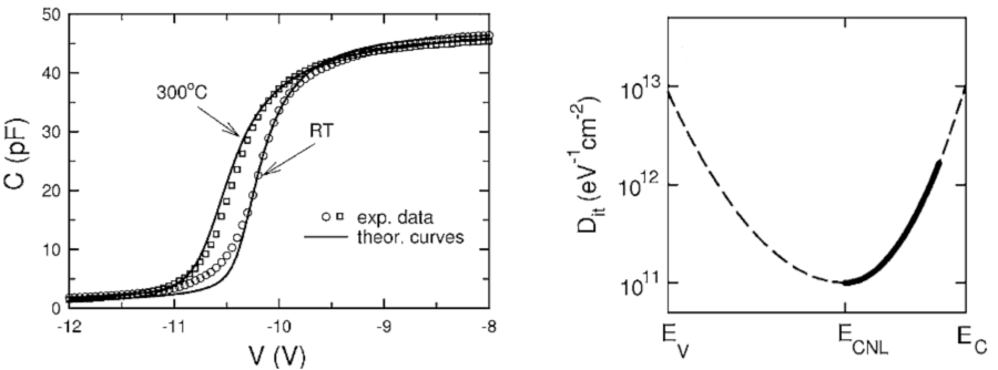

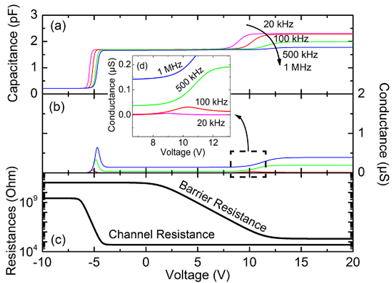

Figure 1.9: (a) A good fit of the CV curves of GaN/AlGaN MIS–HEMTs can be performed assuming a model which includes a major contribution of the interface defects. (b) The density of interface traps can be therefore estimated as  as a the best fitting curve (from [42]). (c) On the
other hand, good agreement with experimental data is found by fitting the impedance characteristics without interface traps, by considering the response of the AlGaN barrier to the small–signal excitation only (from [46]).
as a the best fitting curve (from [42]). (c) On the
other hand, good agreement with experimental data is found by fitting the impedance characteristics without interface traps, by considering the response of the AlGaN barrier to the small–signal excitation only (from [46]).
In order to investigate the interface defects, methods based on stress and recovery transients can be applied. While a stress at negative gate bias highlights the contribution of defects from the buffer, with a positive gate voltage the 2DEG effectively shields the gate stack from what lies underneath. The effect of a transient at forward gate bias is a shift to more positive gate voltage of the transfer characteristic of the MOSFET, or of the capacitance characteristic of a MIS structure [48]. This reflects a certain amount of charge being trapped from the channel into defects during stress. By assuming the trap states to be located at the interface between the AlGaN barrier and the dielectric, the density of active defects is

where  is the total amount of trapped charge,
  the dielectric capacitance,
  the elementary charge and
  the amount of right drift of the device characteristic. This method can also be combined
with optical excitation [49, 50] in order to access states with very large activation energies.
the amount of right drift of the device characteristic. This method can also be combined
with optical excitation [49, 50] in order to access states with very large activation energies.
Results from stress and recovery experiments indicate a very large amount of accessible states at the interface with the dielectric. Several measurements on GaN/AlGaN MIS–HEMTs with various barrier and dielectric thickness and different insulator materials
(SiO , Si
, Si N
N , HfO, AlO) have been compared [51], revealing that the amount of
trapped charge responsible for the positive approaches the theoretical limit of the maximum number of charges available at the
interface, which is given by
, HfO, AlO) have been compared [51], revealing that the amount of
trapped charge responsible for the positive approaches the theoretical limit of the maximum number of charges available at the
interface, which is given by  , the product of dielectric capacitance and applied gate bias, as shown in Fig. 1.10. The larger the dielectric constant, the larger the amount of trapped
electrons for the same stress conditions, therefore the density of defects appears to be larger than the density of available electrons in the vicinity of the AlGaN/dielectric interface.
, the product of dielectric capacitance and applied gate bias, as shown in Fig. 1.10. The larger the dielectric constant, the larger the amount of trapped
electrons for the same stress conditions, therefore the density of defects appears to be larger than the density of available electrons in the vicinity of the AlGaN/dielectric interface.
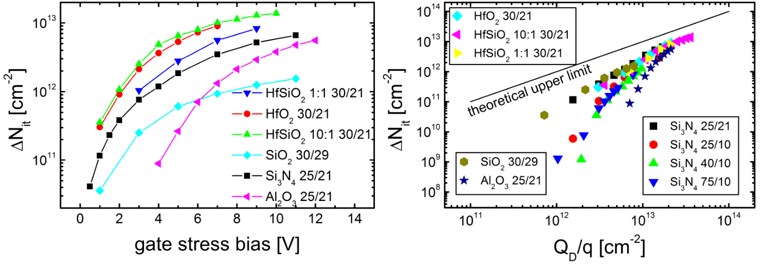

Figure 1.10: (a) The amount of trapped charge increases with stress bias,  , and with the dielectric constant. (b) The amount
of charge present at the gate is
, and with the dielectric constant. (b) The amount
of charge present at the gate is  , and it represents the
maximum amount of charge that can be trapped at the AlGaN/dielectric interface. The amount of traps responsible for the shift get very close to the upper limit in all cases considered in this study (from [51]).
, and it represents the
maximum amount of charge that can be trapped at the AlGaN/dielectric interface. The amount of traps responsible for the shift get very close to the upper limit in all cases considered in this study (from [51]).
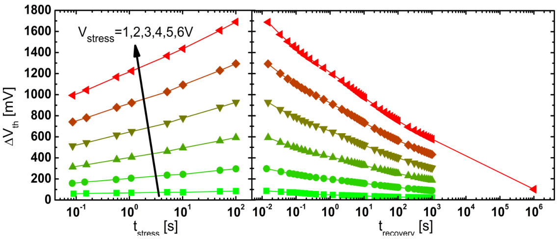
The temporal evolution of the amount of positive drift during stress and recovery allows to understand some of the defect’s properties. For example, the characteristic time constant can be extracted from this kind of measurements. By assuming a physical model for charge trapping, we can calculate from the time constants the activation energy, the defect density and other characteristics of the trap levels, which might contribute to their identification. A broad study of the trapping behavior in GaN/AlGaN MIS–HEMTs under forward gate bias stress indicates that all devices show a linear degradation as a function of the logarithm of time, both during stress and recovery [52], as shown in Fig. 1.11. Similarly to what has been concluded for silicon, this behavior cannot be explained by a unique trap site with a specific time constant [53], but by an ensemble of defects with associated time constant distributed from very short (100 ns) to very large (10 ks) values.
Very recently, a novel surface treatment to the AlGaN layer has been applied before the deposition of the dielectric. This process involving fluorine results in a slightly different 2DEG density at the GaN/AlGaN interface, but also in a fundamentally different trapping behavior at the AlGaN/dielectric interface [54]. In fact, these structures show a relatively high density of defects with a single characteristic time constant of about 100 µs at room temperature. This result indicates that the native surface donor states can be modified with certain chemical processes, and this might be the key to obtain more reliable and stable devices in terms of positive gate bias degradation in future.
A question that still needs a satisfactory answer regards the identity and possible interplay of the surface donor states, responsible for the 2DEG formation, and the states that cause positive shift under forward bias stress. In particular, the exact properties of the surface donor
states can be of fundamental importance. In fact, if we assume that they originate from “deep” defects, i.e., defects with large activation energy and long time constants, they should be usually inactive and apparently stable under normal conditions, but they might
still emit one electron causing a negative shift of the device characteristic. As a consequence, the threshold voltage would also change to a more negative value. This is potentially hazardous in terms of the final application, because it might result in an
unintentional device turn–on.
Further investigations are therefore required in order to fully understand the dynamics of charge trapping and the origin of the 2DEG, which are the driving questions of the present thesis. The charge trapping dynamics will be addressed with further positive gate bias measurements, focusing in particular on the methodology for a reliable characterization method. The question about the origin of the 2DEG can be investigated in two directions: with stress and recovery experiments at very high temperatures, or with the aid of optical excitation. In this work we develop an optical setup that integrates the existing electrical characterization system, allowing to perform measurements under monochromatic light exposure and thus giving us access to defect states with large activation energy.
« PreviousUpNext »ContentsPrevious: 1 Introduction Top: 1 Introduction Next: 1.3 Goal of this thesis