« PreviousUpNext »Contents
Previous: 2.2 Measurement setup Top: 2 Experimental aspects Next: 2.4 Setup for opto-electrical characterization
2.3 Fast measurement with a lock–in amplifier
A Zurich Instruments HF2LI lock–in amplifier has been integrated to the existing experimental facility. Similarly to the impedance analyzer, this instrument can perform impedance measurements, but it offers a much higher time resolution, thus allowing for very fast transients to be recorded.
Generally speaking, lock–in amplifiers are used to measure signals with a known carrier wave. They find their typical application in extracting a signal from a noisy background, provided that the signal is modulated over a known frequency. This instrument can be extremely reliable even when the signal to noise ratio is very poor. The actual ratio between the amplitude of the maximum tolerable noise and that of the signal is called dynamic reserve, and it is expressed in decibel (dB). For the Zurich Instruments HF2LI the dynamic reserve is 100 dB [57], which means that we can measure accurately a signal hundred thousand times smaller than the background noise.
In the following, we describe the working principle of lock–in amplifiers, the phase sensitive detection, and the functionality of our setup in particular. Then we report some details about the calculation of the impedance of the devices under test and, finally, we present our approach to fast sampling measurements .
2.3.1 Functional description
A lock–in amplifier needs a reference signal of a certain frequency, which can be generated by the internal oscillator or provided by an external function generator. In our case, we use the internal oscillator signal as the reference  , a sinusoidal wave with
amplitude
, a sinusoidal wave with
amplitude  V and customizable frequency. The higher
the frequency, the larger are the parasitic effects due to the cables and the probes which contact the device. Above a maximum frequency limit the measurements must be considered not reliable anymore. In our case, the limit is 1 MHz, since our setup
features standard DC probes only.
V and customizable frequency. The higher
the frequency, the larger are the parasitic effects due to the cables and the probes which contact the device. Above a maximum frequency limit the measurements must be considered not reliable anymore. In our case, the limit is 1 MHz, since our setup
features standard DC probes only.
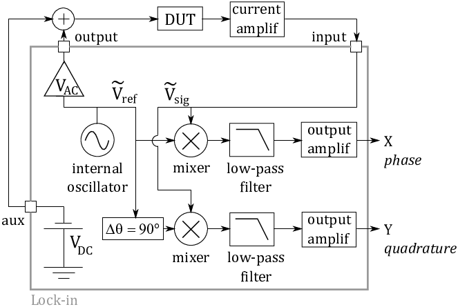


The reference signal is used to generate the output signal to be applied to the device under test (DUT), as illustrated in Fig. 2.4a. Its amplitude  can be adjusted, and we choose typically
50 mV in order to perform small–signal measurements. In addition, the DC baseline of the output signal can be set by using an auxiliary output,
can be adjusted, and we choose typically
50 mV in order to perform small–signal measurements. In addition, the DC baseline of the output signal can be set by using an auxiliary output,  .
.
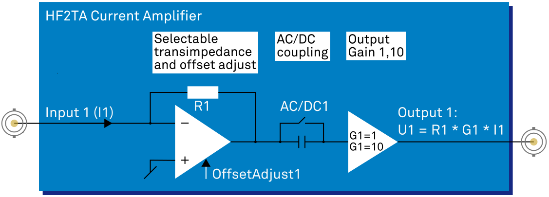
The response of the device is led to a current to voltage amplifier, which is described in Fig. 2.4b. The first part of the amplifier consists of a transimpedance stage, which
converts the input current I1 to a voltage output. The load R1 can be set to one out of seven available values, which determine the gain in a range from 100 V/A to 100 MV/A. A second amplifying stage offers an output voltage gain G1 of one or ten.
In addition, a switch allows to measure the DC signal directly, or to select AC coupling mode, thus removing the DC offset. Finally, an analog to digital converter digitizes the signal into the measured signal,  .
.
In general, the measured signal has the same frequency of the reference, but a different phase  . The core of the lock–in amplifier, the
phase sensitive detector, uses this information in order to extract the signal of interest. Two analog multipliers (or mixers) combine the measured signal with the reference , applying a phase shift of
. The core of the lock–in amplifier, the
phase sensitive detector, uses this information in order to extract the signal of interest. Two analog multipliers (or mixers) combine the measured signal with the reference , applying a phase shift of
 and
and  90°. Performing this operation,
a coefficient
90°. Performing this operation,
a coefficient  1/V is also introduced. We indicate the amplitudes of the measured and reference signals as
 V and
V and  respectively, and their angular frequencies
(
respectively, and their angular frequencies
( ) with
  and
and  . In this way, the result obtained by
mixing is
. In this way, the result obtained by
mixing is

If the two frequencies are different, this procedure is called heterodyne demodulation, the working principle of radio transmissions. However, we expect that the response of the DUT has the same frequency of the excitation ( ), therefore we are performing a homodyne detection. In this case the result is a DC component proportional to the product of the two signals’ amplitudes, plus a component at high frequency
  . In fact, the aim of the lock–in amplifier is to shift the spectrum of the demodulated signal
to base band, i.e., as close to DC as possible. At this point, the desired amplitude can be found by
applying a digital low–pass filter, which can exclude the component from the output of the mixers. In other words, we perform a temporal
average of the two demodulated signals, which brings us to the final outputs of the lock–in amplifier,
. In fact, the aim of the lock–in amplifier is to shift the spectrum of the demodulated signal
to base band, i.e., as close to DC as possible. At this point, the desired amplitude can be found by
applying a digital low–pass filter, which can exclude the component from the output of the mixers. In other words, we perform a temporal
average of the two demodulated signals, which brings us to the final outputs of the lock–in amplifier,  and
and  :
:

These two components, measured in  , describe a vector in the complex plane in
cartesian coordinates: on the real axis, on the imaginary axis. They are called phase and quadrature respectively,
as they represent the part of the signal in phase and out of phase with respect to the reference. In polar coordinates, the same vector
, describe a vector in the complex plane in
cartesian coordinates: on the real axis, on the imaginary axis. They are called phase and quadrature respectively,
as they represent the part of the signal in phase and out of phase with respect to the reference. In polar coordinates, the same vector  is indicated by
  : the amplitude is
  and the phase is
  . The measured signal R
corresponds to the RMS value of the signal amplitude, . Therefore, we can reconstruct the complex
signal
. The measured signal R
corresponds to the RMS value of the signal amplitude, . Therefore, we can reconstruct the complex
signal  as
as

2.3.2 Impedance measurement
The complex vector  can be related to the capacitance and conductance of the DUT.
Indicating with
can be related to the capacitance and conductance of the DUT.
Indicating with  the current flowing from the DUT to the amplifier, we can express it in relation to the
measured signal as
the current flowing from the DUT to the amplifier, we can express it in relation to the
measured signal as

where  is the total gain, and the negative sign
comes from the fact that the current amplifier gives a phase shift of 180°. The current can be also related to the excitation signal applied to the DUT,
is the total gain, and the negative sign
comes from the fact that the current amplifier gives a phase shift of 180°. The current can be also related to the excitation signal applied to the DUT,  and the measured complex impedance
  (or the measured complex admittance
  ) as
) as

Thus, we can calculate the measured impedance in a straightforward way as

and the measured admittance as

At this point, we need to assume an impedance model for the device under test. The complex impedance or admittance are described by a couple of real numbers, which define their real and imaginary parts. We can think of our MIS device (or MIS–HEMT) as
a capacitor, in which displacement currents take place as well. The correct way to describe its behavior is the parallel model: a capacitance  and a conductance
  in parallel. The complex admittance in this case is
given simply by
in parallel. The complex admittance in this case is
given simply by  . Therefore, we find the solution in terms of the lock–in measured quantities and as

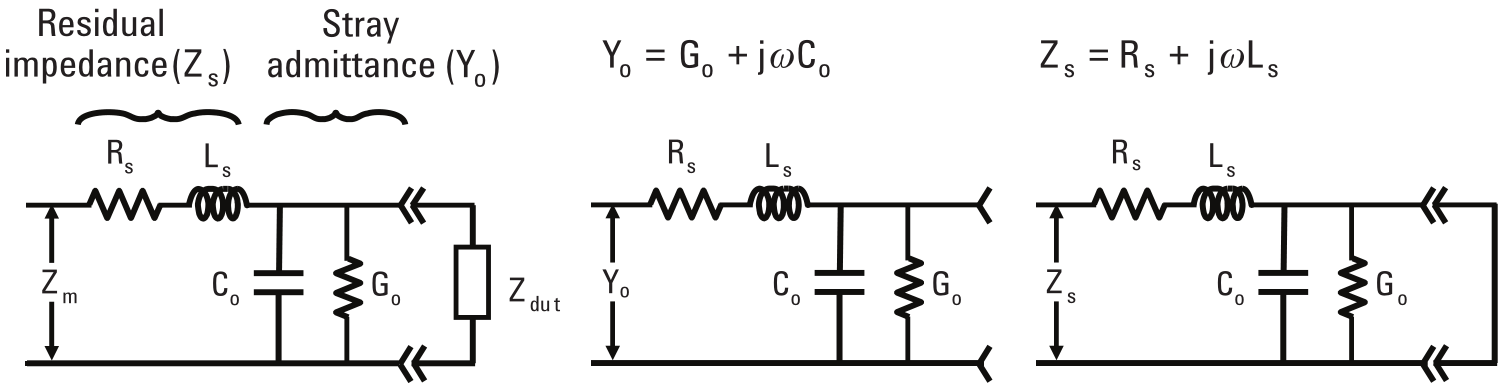

Finally, we can improve our result by correcting the test fixture residuals. In fact, the actual and measurement includes not only the DUT, but also
the probes and the cables necessary for the connection. This introduces a parasitic effect, which can be simplified and modelled as an additional residual impedance  and a stray admittance
  , as shown in Fig. 2.5a. Performing a measurement with open terminals (Fig. 2.5b) and one by contacting the two probes directly together (Fig. 2.5c), we have an estimate of the
parasitic components
, as shown in Fig. 2.5a. Performing a measurement with open terminals (Fig. 2.5b) and one by contacting the two probes directly together (Fig. 2.5c), we have an estimate of the
parasitic components  ,
,  ,
,  and
and  . In this way, we can correct our and to the real DUT capacitance and conductance
 and
and  by solving the following equation for
  :
:

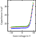
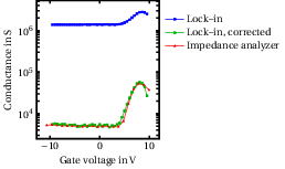
An example of the result achieved by such a correction is shown in Fig. 2.6 for a CV characteristic of a GaN/AlGaN MIS device. A measurement with the impedance analyzer is also included. We clearly see that the parasitics correction leads us to a more accurate measurements, since the result from the lock–in amplifier after correction agrees with that of the impedance analyzer. The difference in shape of the CV curve is due to the different timing of the measurement, and it will discussed in detail in Chapter 3.

2.3.3 Sampling measurement
The main reason to use the lock–in amplifier for impedance measurements is that it offers a very high time resolution. In fact, the sampling rate of this instrument can be as high as 210 MSa/s, and it can be adjusted during operation to fit the user’s
needs. The lower limit is given by the Nyquist principle, which states that the sampling frequency must be at least twice the maximum signal frequency to avoid aliasing. We usually choose a fixed signal frequency  and we tune the sampling rate making sure that it never
falls below
and we tune the sampling rate making sure that it never
falls below  .
.
We set the sampling frequency to a value large enough to achieve the desired time resolution, but not exceeding it further in order to keep an acceptable number of samples. To maximize the resolution at the beginning of the transient, the measurement starts with maximum sampling rate, at the instant when the trigger to the auxiliary output is sent. Then the driving software, included in the main LabView interface, automatically selects the sampling rate to record a constant number of samples per decade. In this way, an approximately logarithmic spacing in time between samples is achieved.
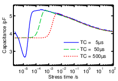
The smallest time at which the lock–in provides an accurate measurement depends on the time constant (TC) of the digital filter. A small TC results in fast sampling, at the expenses of the signal to noise ratio. Therefore, a trade–off must be found in order to perform accurate and fast sampling at the same time. In fact, a certain amount of time is needed for the lock–in to reach the correct final value, which itself depends on the chosen TC. This is due to the roll–off of the digital filter, which is a characteristic depending on the filter order. Before the settling time of the filter, the lock–in response is a convolution of the signal with the filter time response. For example, the fourth order filter in use in our case has a roll–off of 24 dB/octave. In this case, an accuracy of 99% is achieved after ten times the chosen time constant [57]. Therefore, with a TC of 5 µs the time resolution is of approximately 50 µs, for a TC of 50 µs the first accurate point is at 500 µs and so on, as one can see in Fig. 2.7.
Taking into account the points discussed in this section, the lock–in amplifier enables us to measure accurate impedance transients with a time resolution of 50 µs, thus allowing five orders of magnitude more than with the standard impedance analyzer, as shown in Fig. 2.8. This enables us to develop a methodology for characterization of interface defects, which will be the object of Chapter 3.
Previous: 2.2 Measurement setup Top: 2 Experimental aspects Next: 2.4 Setup for opto-electrical characterization