|
|
|
|
Previous: 4.1 Electron Confinement at the Semiconductor-Oxide Interface Up: 4.1 Electron Confinement at the Semiconductor-Oxide Interface Next: 4.1.2 Substrate Orientation (001) |
In the following section the subband structure of electrons confined near the
Si-SiO![]() interface is discussed. As shown in Section 3.4.1 the
conduction band edge of Si is located along the
interface is discussed. As shown in Section 3.4.1 the
conduction band edge of Si is located along the ![]() direction and is
located in the vicinity of the
direction and is
located in the vicinity of the ![]() symmetry point. Each valley is characterized
by a longitudinal mass
symmetry point. Each valley is characterized
by a longitudinal mass
![]() and a transverse mass
and a transverse mass
![]() . In the following
only the three valley pairs along the equivalent
. In the following
only the three valley pairs along the equivalent ![]() axes are
considered, whereas the valleys at the
axes are
considered, whereas the valleys at the ![]() points are neglected. In the
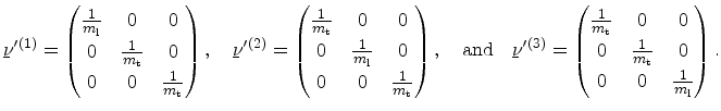
principal crystallographic system the inverse effective mass tensors describing
the energy dispersion of the three valley pairs are given by
points are neglected. In the
principal crystallographic system the inverse effective mass tensors describing
the energy dispersion of the three valley pairs are given by
|
|
|
|
Previous: 4.1 Electron Confinement at the Semiconductor-Oxide Interface Up: 4.1 Electron Confinement at the Semiconductor-Oxide Interface Next: 4.1.2 Substrate Orientation (001) |