|
|
|
|
Previous: 5. Physical Mobility Modeling Up: 5. Physical Mobility Modeling Next: 5.2 Validity of the Boltzmann Transport Equation |
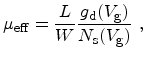
| (5.1) |
In a semiconductor the mobility of electrons is different from that of holes. The reason is the different band structure and scattering mechanisms of these two carrier types. When one charge carrier is dominant the conductivity of a semiconductor is directly proportional to the mobility of the dominant carrier. In Figure 5.1a and 5.1b the electron mobility of Si is plotted. The mobility in Si is a strong function of temperature and impurity concentration.
The device characteristics of MOSFETs is strongly influenced by transport in the inversion layer. Thus, the lattice mobility, representing a bulk quantity, cannot be directly used as a model parameter. In fully depleted silicon-on-insulator (FDSOI) and ultra-thin-body (UTB) MOSFETs all charge carriers reside in the inversion layer, thus quantum confinement and surface roughness scattering have to be taken into account when modeling the mobility.
The low-field mobility in inversion layers, when analyzed as a function of the confining electric field, is a function of doping, gate-voltage, back-bias voltage, and gate oxide thickness. Sabnis and Clemens found that the mobility data shows a universal behavior [Sabnis79], if it is plotted as a function of the effective field
On the basis of this work, investigations for different substrate orientations
were performed. It was found that a similar universal behavior is achieved when
the value of ![]() [Takagi94] is properly adapted.
[Takagi94] is properly adapted.
The first mobility studies were performed on MOSFETs with a spatially uniform
doping profile in the channel. Later on, the validity of the universality of
the effective mobility in channels with arbitrary doping profiles was
investigated. It was discovered that the doping dependence of the effective
mobility can be eliminated if plotted as a function of
![]() , where the coefficient
, where the coefficient ![]() is
sensitive upon the shape of the doping profile [Vasileska97].
is
sensitive upon the shape of the doping profile [Vasileska97].
With the advent of SOI technologies, the physical basis and limitation of the
universal nature of the effective mobility was examined for fully depleted SOI
inversion layers. It was found that the universal mobility behavior does not
hold if the electron density distribution reaches the lower surface of the
Si layer. For such SOI structures with extremely thin Si film thickness
![]() it has been predicted that there exists another kind of
universal mobility behavior as a function of the inversion electron density
it has been predicted that there exists another kind of
universal mobility behavior as a function of the inversion electron density
![]() , independent of the impurity concentration
, independent of the impurity concentration
![]() and
the buried oxide layer thickness
and
the buried oxide layer thickness
![]() [Shoji97].
[Shoji97].
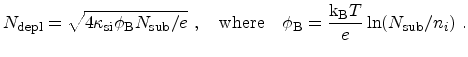
The effective mobility
![]() in Si inversion layers can be experimentally
determined from the drain conductance
in Si inversion layers can be experimentally
determined from the drain conductance
![]() in the linear region
in the linear region
 |
(5.3) |
 |
(5.4) |
Figure 5.2 shows that the mobility characteristics of MOSFET
inversion layers can be split into three distinctive regions. At low inversion
charge densities (low vertical fields), mobility is limited by scattering with
doping atoms and charges at the Si-SiO![]() interface (Coulomb
scattering). Going to higher inversion densities, phonon scattering gains
importance and dominates over Coulomb scattering. At large
interface (Coulomb
scattering). Going to higher inversion densities, phonon scattering gains
importance and dominates over Coulomb scattering. At large
![]() scattering with surface roughness limits the total mobility.
scattering with surface roughness limits the total mobility.
To understand how the different scattering mechanisms affect the performance of
a device on a circuit level, the device switching trajectory in the
![]() -
-
![]() space has to be considered. It has been found that for the delay
of a ring oscillator the mobility at low and intermediate
space has to be considered. It has been found that for the delay
of a ring oscillator the mobility at low and intermediate
![]() is important,
because there the device spends comparatively more time than in the high gate
field region [Mujtaba95].
is important,
because there the device spends comparatively more time than in the high gate
field region [Mujtaba95].
|
|
|
|
Previous: 5. Physical Mobility Modeling Up: 5. Physical Mobility Modeling Next: 5.2 Validity of the Boltzmann Transport Equation |
![\includegraphics[width=0.495\textwidth]{xcrv-scipts/ExpMob.eps}](img808.png) [b]
[b]![\includegraphics[width= 0.495\textwidth]{xcrv-scipts/ExpMobNd.eps}](img809.png)
![\includegraphics[scale=1.0, clip]{inkscape/SchematicEffmob.eps}](img831.png)