


Next: 5.1.4 Poly Silicon Structures
Up: 5.1 Fabrication Techniques
Previous: 5.1.2 Step Edge Cut
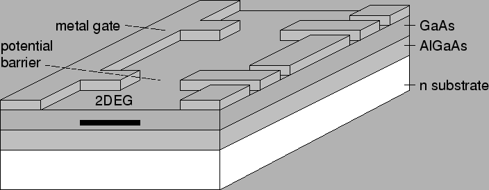
A commonly studied structure is a planar quantum dot [67]
[68] [85] [86], which is created by
lateral patterning of several metal electrodes, or gates, on the surface
of a two-dimensional electron gas. Often the heterostructure is formed
by GaAs/AlGaAs layers, as shown in Fig. 5.3.
Figure 5.3:
Laterally patterned two-dimensional electron gas in a semiconductor
heterostructure. The fingers can be biased individually, which allows an
independent change of barrier heights.
 |
Semiconductor quantum dots show richer characteristics, due to their
larger energy level spacing. Interesting is, that the individual barrier
heights are tunable by changing the finger electrode potentials. This is
used to operate an oscillating-barrier turnstile [85] [107],
where the first barrier is lowered to let one electron pass into the quantum
dot. Then this barrier is raised and the second barrier is lowered to let
the electron exit the quantum dot. Electrons are passed turnstile like
through the device.
A different approach to realizing single-electron tunneling in semiconductors is to
have current flow vertically with respect to heterostructure layers.
The heterostructure layers provide vertical confinement and lithography
defines in-plane confinement.
Next: 5.1.4 Poly Silicon Structures
Up: 5.1 Fabrication Techniques
Previous: 5.1.2 Step Edge Cut
Christoph Wasshuber