


Next: 5.2 Single Electron Memories
Up: 5.1 Fabrication Techniques
Previous: 5.1.4 Poly Silicon Structures
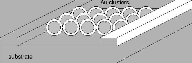
Finally we want to mention linked gold clusters [6] [55]
[93]. Here a totally different approach of fabrication is
followed. Instead of patterning or depositing material on a substrate,
gold clusters, with a diameter in range from 1-20 nm with a narrow size
distribution, covered with an organic layer are manufactured first. These
clusters are then spread on a surface, as shown in Fig. 5.5,
and linked with molecular wires, consisting of conductive organic molecules.
Figure 5.5:
Array of linked gold clusters. The gold clusters are grown as
aerosol particles, annealed, spread on a surface and linked with molecular
wires.
 |
The metal clusters are grown as aerosol particles in a gas aggregation
reactor and are annealed in flight to yield perfect single crystal particles.
An appealing feature is that this technique is close to an impurity and
defect free production, which is, due to the extreme charge sensitivity
of single-electron devices, a big advantage.
Christoph Wasshuber