In the following two examples are presented which have been part of simulation projects carried out at the Institute for Microlectronics. For both an anisotropic refinement strategy was required to create mesh points in a small region under a particular surface, which was necessary for further simulations. The layer refinement method presented in Section 3.2 in combination with the gradient refinement method presented in Section 3.3 was used to obtain the results presented in the following.
For a typical semiconductor process step, the surfaces of the structure are
in general non-planar [64]. This example demonstrates that the surface
distance transform strategy also works for curved surfaces.
Figure 3.17 shows the initial, regular coarse mesh. The aerial
surface is again covered by a mask (blue). For the refinement strategy a
gradient driven anisotropic approach in combination with an approximation of
the surface distance transform is selected with respect to the solution of
Laplace equation, where the boundary conditions are set as follows. The
upper surface which is not covered by the blue mask carries a Dirichlet
condition with the value ![]() and the opposite bottom faced surface is
set to 0
. At all other surfaces Neumann boundary conditions
are applied. For the dilation function the analytical form as plotted in
Figure 3.6 is chosen.
and the opposite bottom faced surface is
set to 0
. At all other surfaces Neumann boundary conditions
are applied. For the dilation function the analytical form as plotted in
Figure 3.6 is chosen.
![\includegraphics[width=0.47\textwidth]{pics/nps_coarse.eps2}](img294.png)
|
![\begin{figure*}
% latex2html id marker 3111
\setcounter{subfigure}{0}
\centering...
...dra.]
{\epsfig{figure =pics/nps_fine.eps2,width=0.47\textwidth}}\end{figure*}](img295.png) |
The resulting mesh after refinement can be seen in Figure 3.18(b). Due to the fact that the solution of the Laplace equation is only an approximation for the surface distance function, the refinement layer covers surface-near regions with different thickness, which is acceptable regarding the small computational effort calculating the Laplace equation compared to a real surface distance transform calculation. The anisotropy is distinct and reflects excellently the gradient direction.
Due to the growing complexity of modern semiconductor device structures,
especially in the field of non-volatile memories, but also in the field of
classical CMOS technology three-dimensional semiconductor process simulation
gradually gains more importance. The focus for this example is on non-volatile
memories (NVM) which play an important role in modern system on chip solutions.
This example shows an anisotropic refinement result of the simulation domain of
an EEPROM memory cell which has been developed by J.M.
Caywood [65]. The cell was part of a full manufacturing cycle
simulation, followed by the extraction of the coupling
capacitance [66]. Such a kind of analysis allows to optimize the layout
of the EEPROM memory cell as well as the process parameters. To improve the
accuracy anisotropic mesh refinement was applied in the field oxide region
of the cell. The results of this refinement procedure are presented in the
following.
For the simulation of the Caywood-EEPROM memory cell, seven simulation steps
had to be performed. The simulation starts with the oxidation of the field
oxide. Due to the two-dimensional nature of this problem, this simulation step
was carried out with DIOS-ISE [67].
By addition of the floating gate to the
structure, the actual three-dimensional simulation starts. All other simulation
steps related to the gate forming process have been carried out with
TOPO3D [68], which is a topography simulator developed at the
Institute for Microlectronics. For the three-dimensional simulation cycle only a small part of the
whole EEPROM cell is used due to a highly symmetric
constellation. Figure 3.19 gives the aerial image simulation result
of the floating gate mask of a ![]() cell array. The rectangular
region marks the actual simulation domain.
cell array. The rectangular
region marks the actual simulation domain.
![\includegraphics[width=0.7\columnwidth]{pics/aerial.eps2}](img296.png)
|
Figure 3.20(a) and Figure 3.20(b), respectively, show a
comparison between the simulation domain and a scanning electron microscope
(SEM) picture of the floating gate structure before the floating gate is
covered by a small oxide isolation layer. Figure 3.20(c) gives an
overview of all considered regions and the used materials.
![\begin{figure*}\setcounter{subfigure}{0}
\centering
\subfigure[Full simulation d...
...on domain.]
{\epsfig{figure =pics/t3.eps,height=0.4\textwidth}}
\end{figure*}](img297.png) |
Starting from the structure depicted in Figure 3.20(a) for the next
simulation step, namely the oxidation of a thin isolation layer between the two
gates in the EEPROM cell, a small layer with higher mesh density involving the
surface which is exposed to an oxidizing atmosphere has to be generated.
Oxidation, by the means of a process step as part of the fabrication of
integrated circuits (IC), is a directional and surface near process. Based on
this note the refinement should be anisotropic. Higher mesh densities
arise perpendicular to the surface and should influence only a thin layer. To
accomplish this task, a gradient refinement method, see
Section 3.3, in combination with the layer refinement method,
discussed in Section 3.2, is a good choice.
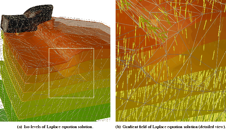 |
For the layer refinement method again the Laplace equation is used to calculate an
approximation of the surface distance field. Since the granularity of the mesh
in the floating gate region exhibits an appropriate density, only the surface
of the field oxide region should be refined. Figure 3.21(a) shows
iso-levels of the solution of the Laplace equation, where for the boundary
conditions the upper silicon dioxide surface was set to ![]() and the opposite
part of the silicon body was set to 0
. For the Laplace
equation the wafer and the field oxide domain form one common structure, so
that there are no interface conditions applied between silicon and silicon
dioxide. All other surfaces carry Neumann boundary conditions.
and the opposite
part of the silicon body was set to 0
. For the Laplace
equation the wafer and the field oxide domain form one common structure, so
that there are no interface conditions applied between silicon and silicon
dioxide. All other surfaces carry Neumann boundary conditions.
Figure 3.21(b) shows the corresponding gradient field of
the Laplace equation solution. For the dilation function which is used for the
layer/gradient refinement method again a Gaussian bell curve shaped function is
applied to limit the refined regions to values of approximately ![]() from the
maximum of the Laplace equation solution, cf. Figure 3.6.
from the
maximum of the Laplace equation solution, cf. Figure 3.6.
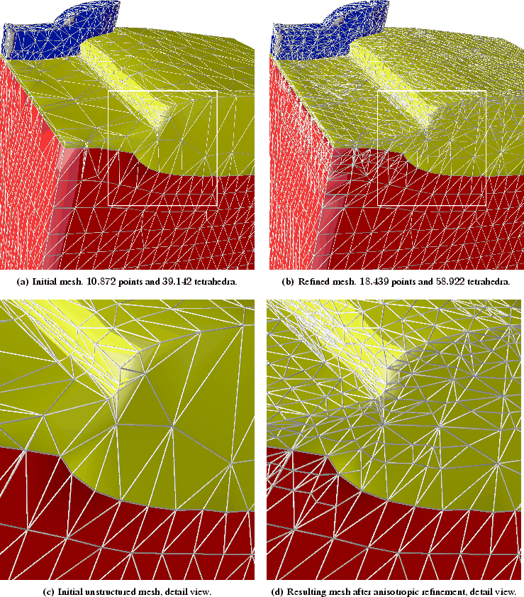
Figure 3.22(c) and Figure 3.22(d) show a detailed view of the initial coarse and the refined mesh structure, whereby the initial mesh as part of the refined mesh can clearly be observed. The refinement is anisotropic so that small mesh point distances perpendicular to the surface are obtained. The surface directional mesh density is only influenced by the anisotropic tetrahedral bisection algorithm presented in Table 2.2.
 |