While most of the miniaturization problems in CMOS technology are more or less related to doping issues, the continued reduction of the gate oxide thickness has necessitated the incorporation of nitrogen into silicon dioxide, which in turn has aggravated NBTI (negative bias temperature instability), especially, since we have entered the 90nm and 65nm technology nodes. As drive currents increase HCI reliability usually gets worse since the drive current directly determines the carriers generated by impact ionization. However, optimization of the drain extension doping profile reduces the electric field at the drain edge significantly. Therefore, the substrate current, which is a quantitative measure for impact ionization, is strongly reduced for advanced CMOS technologies [115]. Since HCI has lost on importance and NBTI is the leading reliability concern for current technology nodes, a detailed analysis of the degradation and relaxation behavior of the NBTI mechanism in a 90nm transistor is presented.
The key device parameters of the p-MOSFET such as threshold voltage and
saturation current show a rapid shift under negative bias at an elevated
temperature due to the build-up of positive interface charges. Since indirect
measuring techniques have to be applied, it is difficult to correlate
measurement results to NBTI induced degradation of the gate-dielectric/substrate
interface associated with bond breaking and chemical species. While the exact
nature of the complex NBTI mechanism is still unknown, it is widely accepted
that interface traps are generated by breaking of hydrogen-passivated silicon
bonds at the interface and subsequent diffusion of
hydrogen [116,117,25]. Charge pumping and gate
leakage current measurements revealed that NBTI under moderate oxide fields
is purely due to interface traps ![]() and the generated oxide traps
and the generated oxide traps
![]() can be neglected [118]. The NBTI induced interface
charges cause a parameter degradation of the MOSFET firstly due to a reduction
in inversion layer holes and secondly due to a mobility degradation by Coulomb
scattering. Both the reduced gate overdrive
can be neglected [118]. The NBTI induced interface
charges cause a parameter degradation of the MOSFET firstly due to a reduction
in inversion layer holes and secondly due to a mobility degradation by Coulomb
scattering. Both the reduced gate overdrive
![]() and
the degraded mobility reduce the saturation current and the transconductance
of the transistor.
and
the degraded mobility reduce the saturation current and the transconductance
of the transistor.
Jeppson and Svensson studied the process of trap formation at the
Si/SiO
![]() interface during NBT stress in MOS
capacitors in 1977 [119]. They found that the NBTI-driven shift of
the threshold voltage in p-MOSFETs depends on the applied gate voltage,
temperature, and stress time. It is commonly assumed that the generated
interface states are dangling silicon bonds with an energy distribution
within the silicon band gap. Holes can occupy these energy states under
inversion condition and produce positive interface charges [116].
For advanced CMOS technologies, nitrogen is incorporated in thinner gate oxides
mainly to reduce gate leakage current, to avoid boron penetration into the
dielectric, and to improve HCI reliability. However, it turned out that
silicon dioxide-nitride compositions exhibit a significantly higher NBTI
degradation compared to pure silicon dioxide for the same physical oxide
thickness and voltage condition [13]. Experimental studies revealed
that the thermal activation energy of interface trap generation decreases
steadily with increasing nitrogen concentration at the interface [120,121].
interface during NBT stress in MOS
capacitors in 1977 [119]. They found that the NBTI-driven shift of
the threshold voltage in p-MOSFETs depends on the applied gate voltage,
temperature, and stress time. It is commonly assumed that the generated
interface states are dangling silicon bonds with an energy distribution
within the silicon band gap. Holes can occupy these energy states under
inversion condition and produce positive interface charges [116].
For advanced CMOS technologies, nitrogen is incorporated in thinner gate oxides
mainly to reduce gate leakage current, to avoid boron penetration into the
dielectric, and to improve HCI reliability. However, it turned out that
silicon dioxide-nitride compositions exhibit a significantly higher NBTI
degradation compared to pure silicon dioxide for the same physical oxide
thickness and voltage condition [13]. Experimental studies revealed
that the thermal activation energy of interface trap generation decreases
steadily with increasing nitrogen concentration at the interface [120,121].
Under dynamic operation of the transistor the interface traps which are
generated during the on-state are partially annealed in the off-state. Therefore
the AC degradation is significantly lower than the DC degradation for any given
stress time. The magnitude of the NBTI driven parameter shift over time is
significantly reduced for higher frequencies [122] or smaller
``on''duty cycles [123,124]. In this section we analyze
mainly the impact of an operation at higher frequencies in the MHz-range at
slightly different supply voltages on the AC lifetime of a 90nm transistor.
The NBTI transistor level degradation is closely linked to circuit and product
level degradation, which will be analyzed for a typical 90nm-based SRAM memory
cell in Section 6.4.
![\resizebox{0.945\linewidth}{!}{\rotatebox{0}{\includegraphics[clip]{figures/nbti-exp-comb}}}](img542.png)
|
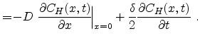
The sketch on the left hand side of Fig. 5.1 shows the used configuration
for NBTI experiments under DC and AC gate voltage stress conditions at a constant
temperature of 125![]() C. The used amplitude for AC stress is identical to the
negative DC voltage during the pulse ``on'' phase and zero Volt during the pulse
``off'' phase. The NBT stress was interrupted at certain times to measure the
threshold voltage and drain saturation current. The threshold voltage
C. The used amplitude for AC stress is identical to the
negative DC voltage during the pulse ``on'' phase and zero Volt during the pulse
``off'' phase. The NBT stress was interrupted at certain times to measure the
threshold voltage and drain saturation current. The threshold voltage ![]() was
extracted by using a linear extrapolation of
was
extracted by using a linear extrapolation of ![]() -
- ![]() data from
the point of maximum transconductance, and the saturation current
data from
the point of maximum transconductance, and the saturation current ![]() was
determined at
was
determined at
![]() and
and
![]() .
.
The measuring interval of the tester used for monitoring the key parameters of the
MOSFET over the stress time should be kept as short as possible to minimize the
influence of relaxation on measurement results. The diagram on the right hand
side of Fig. 5.1 illustrates that the ![]() parameter shift is
significantly reduced by stronger annealing of interface traps for longer
relaxation phases. In the long stress time regime the influence of the relatively
short measuring intervals plays a secondary role and the results of long and short
intervals become comparable. The longer measuring interval lasts ten times longer
than the shorter interval of 700ms.
parameter shift is
significantly reduced by stronger annealing of interface traps for longer
relaxation phases. In the long stress time regime the influence of the relatively
short measuring intervals plays a secondary role and the results of long and short
intervals become comparable. The longer measuring interval lasts ten times longer
than the shorter interval of 700ms.
The accomplishment of all presented NBTI measurements in this section were
managed by Dr. Puchner at Cypress Semiconductor Corp. in San Jose.
Different rectangular gate signals were used in order to analyze the gate
voltage, duty cycle, and frequency dependence of the NBTI degradation behavior.
Voltages were applied from -1.5V down to -2.7V to the gate of
the transistor, frequencies were used in the range from DC to 1MHz, and
``on'' duty cycles in the range of 30% to 70%. The MOSFET parameters ![]() and
and ![]() were monitored for a maximum stress time of
were monitored for a maximum stress time of
![]() s.
The experimental data were used to analyze the relationship between the
s.
The experimental data were used to analyze the relationship between the
![]() shift and the
shift and the ![]() shift, to empirically investigate the gate
voltage and frequency dependence of NBTI, and finally to calibrate the
numerical simulations for the 90nm p-MOSFET device.
shift, to empirically investigate the gate
voltage and frequency dependence of NBTI, and finally to calibrate the
numerical simulations for the 90nm p-MOSFET device.
![\resizebox{1.0\linewidth}{!}{\rotatebox{0}{\includegraphics[clip]{figures/nbti-model-schematic-comb}}}](img552.png)
|
Equation (5.1) states that the ![]() generation is determined by a
chemical hydrogen release reaction with a constant dissociation rate
generation is determined by a
chemical hydrogen release reaction with a constant dissociation rate ![]() , when
the p-MOSFET is biased in inversion. When the transistor is switched off, the
forward rate
, when
the p-MOSFET is biased in inversion. When the transistor is switched off, the
forward rate ![]() becomes zero and the reverse rate
becomes zero and the reverse rate ![]() stays unchanged.
The parameter
stays unchanged.
The parameter ![]() denotes the total Si-H bond density at the interface
before stress. Equation (5.2) is obtained by integration of the standard
diffusion equation across the silicon/oxide interface with a
thickness
denotes the total Si-H bond density at the interface
before stress. Equation (5.2) is obtained by integration of the standard
diffusion equation across the silicon/oxide interface with a
thickness ![]() . The diffusion coefficient
. The diffusion coefficient ![]() is the average diffusivity of
the diffusing hydrogen species (atomic and molecular hydrogen). Note that the
generated interface traps
is the average diffusivity of
the diffusing hydrogen species (atomic and molecular hydrogen). Note that the
generated interface traps ![]() are equal to the number of released hydrogen
atoms at any given time
are equal to the number of released hydrogen
atoms at any given time ![]() .
.
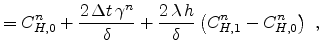
The left sketch in Fig. 5.2 shows that released hydrogen diffuses into
the gate oxide during NBT stress and returns back to the interface when stress
is removed. The active region of the NBTI mechanism is uniformly distributed over
the channel according to a one-dimensional problem. The right sketch depicts that
a hole can tunnel to a Si-H bond during inversion of the p-MOSFET and it can take
one electron of the covalent bonding away. After that, the hydrogen atom diffuses
away with its electron and leaves a positively charged interface trap behind.
The discretization of the differential equations (5.1) and
(5.2) is based on a one-dimensional finite differences method.
The simulation domain for the diffusing hydrogen is the gate oxide with the
boundary condition of an adjustable reflecting and absorbing wall at the
oxide/poly interface. The differential quotients are approximated with
differences using the spatial and temporal increments ![]() and
and ![]() ,
respectively. Grid points
,
respectively. Grid points
![]() with resolution
with resolution
![]() are used for an oxide thickness
are used for an oxide thickness ![]() , and
, and
![]() for
for
![]() and
and
![]() for
for
![]()
We are solving for the next time step
![]() in order to
calculate the hydrogen diffusion profile
in order to
calculate the hydrogen diffusion profile
![]() and the interface trap concentration
and the interface trap concentration
![]() at the
next instant according to the following equations:
at the
next instant according to the following equations:
Fig. 5.3 compares the numerical solution of the calibrated R-D model for
DC and AC operation to experimental data of the investigated 90nm p-MOSFET. The ![]() degradation under static and dynamic NBT stress was simulated with the same model
parameter set, which includes
degradation under static and dynamic NBT stress was simulated with the same model
parameter set, which includes
![]() ,
,
![]() ,
,
![]() ,
and
,
and
![]() nm.
nm.
Chakravarthi et al. found that the atomic hydrogen model exhibits the typical
power-law time dependence
![]() whereas the molecular
hydrogen model predicts a time dependence of
whereas the molecular
hydrogen model predicts a time dependence of ![]() [117].
We found a time exponent of 0.183 for our DC data, which supports that both
atomic and molecular hydrogen is present. The hydrogen distribution is calculated
in the gate oxide with a physical thickness
[117].
We found a time exponent of 0.183 for our DC data, which supports that both
atomic and molecular hydrogen is present. The hydrogen distribution is calculated
in the gate oxide with a physical thickness
![]() nm for
every time step. The final simulation result is the defect density
nm for
every time step. The final simulation result is the defect density ![]() and
the corresponding shift
and
the corresponding shift
![]() .
Fig. 5.4 demonstrates that the calibrated model can be used to study the
evolution of the MOSFET parameter degradation over time under DC and symmetric AC
operation. The dynamic NBTI effect guarantees, even for a very slow switching
operation, that the NBTI lifetime is improved by at least a factor of 2.
.
Fig. 5.4 demonstrates that the calibrated model can be used to study the
evolution of the MOSFET parameter degradation over time under DC and symmetric AC
operation. The dynamic NBTI effect guarantees, even for a very slow switching
operation, that the NBTI lifetime is improved by at least a factor of 2.
The left diagram in Fig. 5.5 shows four snapshots of hydrogen profiles
![]() during the first stress phase. After 400s the transistor
is switched off. The right diagram shows the corresponding profiles during
relaxation. When relaxation starts, the free hydrogen near the interface can
rapidly anneal broken Si-H bonds. The consumption of hydrogen near the interface
creates a diffusion hole. Fig. 5.6 shows the second stress-relaxation
cycle. When stress is applied again, a rapid generation of interface traps starts.
After the diffusion hole is filled the generation slows down due to diffusion
limited transport. In the relaxation phase hydrogen moves back to the interface
again. This forward and backward movement continues in subsequent cycles.
during the first stress phase. After 400s the transistor
is switched off. The right diagram shows the corresponding profiles during
relaxation. When relaxation starts, the free hydrogen near the interface can
rapidly anneal broken Si-H bonds. The consumption of hydrogen near the interface
creates a diffusion hole. Fig. 5.6 shows the second stress-relaxation
cycle. When stress is applied again, a rapid generation of interface traps starts.
After the diffusion hole is filled the generation slows down due to diffusion
limited transport. In the relaxation phase hydrogen moves back to the interface
again. This forward and backward movement continues in subsequent cycles.
![\resizebox{1.0\linewidth}{!}{\rotatebox{0}{\includegraphics[clip]{figures/pic-dynamic}}}](img591.png)
|
![\resizebox{1.0\linewidth}{!}{\rotatebox{0}{\includegraphics[clip]{figures/pic-demo}}}](img592.png)
|
![\resizebox{0.9\linewidth}{!}{\rotatebox{0}{\includegraphics[clip]{figures/pic-cycle1-comb}}}](img593.png)
|
![\resizebox{0.9\linewidth}{!}{\rotatebox{0}{\includegraphics[clip]{figures/pic-cycle2-comb}}}](img594.png)
|
Interface traps are built up quickly during the first seconds of a stress phase
(reaction-limited regime). With increasing time the hydrogen diffusion front
moves towards the oxide-poly interface (diffusion-limited regime). After long
times, free and bounded hydrogen densities at the silicon-oxide interface become
very low, corresponding to a high level of generated interface defects.
Recently, Tsujikawa and Yugami have investigated released hydrogen atoms from
the substrate interface during NBT stress in a p-MOSFET with a 1.85nm thick
nitrided gate dielectric [8]. Although it was expected that
hydrogen can easily diffuse out in the case of ultra-thin gate dielectrics,
it was found that much of the released hydrogen remains in the gate dielectric.
The R-D model must take the accumulation of hydrogen in the gate oxide as
well as the loss of hydrogen into the poly into account in order to predict
the long-time degradation slope appropriately. We suggest to model the
boundary condition at the oxide/poly interface with a more reflecting than
absorbing wall. The simulated accumulation of hydrogen after 400s can be
observed in the right diagram of Fig. 5.5, since the diffusion front
has already reached the poly interface at ![]() nm at this time.
nm at this time.
The effect of an arbitrary space charge ![]() distributed over an interface
zone of thickness
distributed over an interface
zone of thickness ![]() is equivalent to a virtual sheet charge
is equivalent to a virtual sheet charge
![]() located at the silicon/oxide interface according to
located at the silicon/oxide interface according to
![\resizebox{1.0\linewidth}{!}{\rotatebox{0}{\includegraphics[clip]{figures/pic-degout}}}](img608.png)
|
The mobility degradation is primarily large at gate voltages close to ![]() and
affects also the
and
affects also the ![]() shift of the device. A device model is used to derive the
relationship between
shift of the device. A device model is used to derive the
relationship between ![]() shift and trap density
shift and trap density ![]() in a simplified
manner [9].
In the following derivation, the absolute values of quantities are specified to
describe the p-MOSFET and the subscript ``0'' denotes the initial value of a
quantity before stress. The
in a simplified
manner [9].
In the following derivation, the absolute values of quantities are specified to
describe the p-MOSFET and the subscript ``0'' denotes the initial value of a
quantity before stress. The ![]() shift caused by interface traps can be composed
by an electrostatic part and a mobility degradation part:
shift caused by interface traps can be composed
by an electrostatic part and a mobility degradation part:
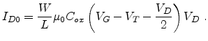
The pre-stress drain current is given by the well-known expression for the linear MOSFET region
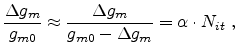
If uniformly distributed interface traps ![]() are introduced, they will
cause a drain current degradation firstly due to a loss in mobile charge and
secondly due to a degradation in mobility, which results in
are introduced, they will
cause a drain current degradation firstly due to a loss in mobile charge and
secondly due to a degradation in mobility, which results in
The mobility degradation caused by Coulomb scattering can be empirically
modeled with a constant ![]() according to
according to
When the degradation of the transconductance ![]() is relatively small, the
relative degradation
is relatively small, the
relative degradation
![]() can be approximated by
can be approximated by
The result
![]() in equation (5.14) is obtained by
differentiating equation (5.11) and (5.12).
in equation (5.14) is obtained by
differentiating equation (5.11) and (5.12).
Since the threshold voltage ![]() is defined for a fixed drain current
is defined for a fixed drain current ![]() in
this derivation,
in
this derivation,
![]() is the difference in the gate voltage after and
before NBT stress. From (5.11) to (5.14) we obtain finally an extended
relationship between
is the difference in the gate voltage after and
before NBT stress. From (5.11) to (5.14) we obtain finally an extended
relationship between
![]() and
and ![]()
where the first term accounts for the reduced inversion charge and the second
term for the mobility degradation. The degraded p-MOSFET has a reduced
transconductance, ![]() , and hence a larger gate voltage
, and hence a larger gate voltage ![]() is required in
order to reach the current level
is required in
order to reach the current level ![]() which defines the threshold voltage.
This results in a contribution by the mobility degradation,
which defines the threshold voltage.
This results in a contribution by the mobility degradation,
![]() , on the total
, on the total ![]() -shift
-shift
![]() .
.
The NBTI driven device parameter shift (![]() ,
, ![]() ) over time depends
significantly on the frequencies and ``on'' duty cycles which are used to drive
the transistor gate. It will be shown that apart from the rectangular waveform
characteristics of the gate signal the supply voltage tolerance of the chip
plays also a major role for the transistor lifetime at a given temperature.
) over time depends
significantly on the frequencies and ``on'' duty cycles which are used to drive
the transistor gate. It will be shown that apart from the rectangular waveform
characteristics of the gate signal the supply voltage tolerance of the chip
plays also a major role for the transistor lifetime at a given temperature.
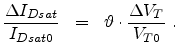
Fig. 5.9 shows the impact of AC operation on the drive current
degradation of the transistor. Note that the 1 : 1 relation between the relative
changes of ![]() and
and ![]() parameters implies an equal relative degradation
level for both parameters.
parameters implies an equal relative degradation
level for both parameters.
![\resizebox{1.0\linewidth}{!}{\rotatebox{0}{\includegraphics[clip]{figures/pic-drive}}}](img630.png)
|
![\resizebox{1.0\linewidth}{!}{\rotatebox{0}{\includegraphics[clip]{figures/pic-drivedyn2}}}](img631.png)
|
![\resizebox{1.0\linewidth}{!}{\rotatebox{0}{\includegraphics[clip]{figures/pic-cmp-frequ}}}](img632.png)
|
![\resizebox{1.0\linewidth}{!}{\rotatebox{0}{\includegraphics[clip]{figures/pic-cmp-dc}}}](img633.png)
|
![\resizebox{1.0\linewidth}{!}{\rotatebox{0}{\includegraphics[clip]{figures/pic-frequ-long}}}](img640.png)
|
![\resizebox{1.0\linewidth}{!}{\rotatebox{0}{\includegraphics[clip]{figures/pic-ext}}}](img641.png)
|
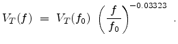
The lifetime extension of the p-MOSFET under higher frequency operation is
analyzed quantitatively in Fig. 5.15. The lifetime at a typical power supply
of 1.45V and a frequency of 10MHz is ten times higher than the DC lifetime.
Due to the high voltage sensitivity of NBTI the impact of a power supply tolerance
of
![]() is investigated. The device lifetime is defined here by
a
is investigated. The device lifetime is defined here by
a ![]() shift of 80mV. The simulation predicts that the AC lifetime at 10MHz lies
between six times (for 1.5V supply) and twenty times (for 1.4V) of the DC lifetime
at 1.45V operation. A remarkable result is also that the lowering of the 1.5V
supply by only 50mV improves the NBTI lifetime by a factor of 1.8.
shift of 80mV. The simulation predicts that the AC lifetime at 10MHz lies
between six times (for 1.5V supply) and twenty times (for 1.4V) of the DC lifetime
at 1.45V operation. A remarkable result is also that the lowering of the 1.5V
supply by only 50mV improves the NBTI lifetime by a factor of 1.8.
The NBTI mechanism was systematically investigated for a 90nm CMOS technology in this section. Experiments for different gate voltages, frequencies, and duty cycles were performed in cooperation with Cypress to analyze the device parameter degradation of the p-MOSFET. It turned out that the R-D model is well suited to explain static and dynamic experimental data. The gate voltage and frequency dependence of NBTI was included by means of an empirical relationship. All measured data could be well reproduced by the performed numerical simulations. The presented simulation approach allows, on a physically rigorous basis, to predict the p-MOSFET lifetime which depends strongly on the applied stress conditions.


![$\displaystyle I_{D} = \frac{W}{L} \mu \left[ C_{ox} \left( V_G - V_T - \frac{V_D}{2} \right) - q N_{it} \right] V_D .$](img612.png)
![$\displaystyle \Delta V_T = \left[\frac{q}{C_{ox}} + \frac{\alpha \!L \!I_T}{W \mu_0 C_{ox} V_D} \right] \cdot N_{it} ,$](img621.png)
![\resizebox{1.0\linewidth}{!}{\rotatebox{0}{\includegraphics[clip]{figures/pic-frequ}}}](img635.png)
![\resizebox{1.0\linewidth}{!}{\rotatebox{0}{\includegraphics[clip]{figures/pic-voltage}}}](img639.png)