Interconnect Reliability
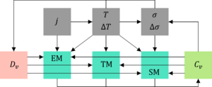
Interconnect is a term given to any conductive layer (most often metal) which is used in integrated circuits (ICs) to electrically contact different devices or chips. The size of these layers can be in the nanometer range, used to contact to the transistors themselves during back end of line (BEOL) fabrication or in the micrometer range, used to stack wafers with different functionalities together through two-and-a-half dimensional (2.5D) or three-dimensional (3D) integration. The main reliability concern of metallization is the accumulation of vacancies, which leads to void formation and increased stress. The forces which bring about the movement of these vacancies – or alternatively the movement of the metal atoms – are summarized by electro-migration (EM), thermo-migration (TM), and stress-migration (SM). The interplay between these driving forces, together with current (j), temperature (T), and stress (σ), and the atomic diffusivity (Dv), brings about a change in the vacancy concentration (Cv), as shown in Fig. 1.
Nano-Interconnects
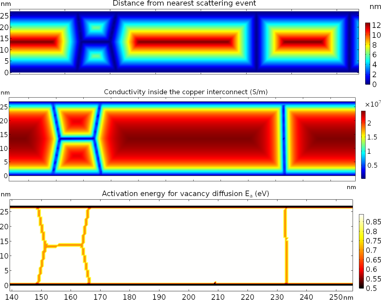
The continued transistor scaling has been bolstered by a simultaneous scaling of the metal interconnects. These shrinking connections can give rise to undesired effects such as increased resistivity and current density, resulting in a reduced interconnect lifetime. When the thickness of a metal layer is reduced, the average crystal grain size decreases almost linearly. This grain size decrease and the overall reduction in thickness means that the grain boundaries and material interfaces play an increasingly important role in the conductive and reliability behavior of interconnects. We are able to model the reliability of thin metal layers down to the nanoscale, while taking into consideration the granular microstructure. This is achieved by treating all relevant parameters, such as conductivity (Fig. 2) and vacancy diffusivity as spatial material parameters.
3D Integration
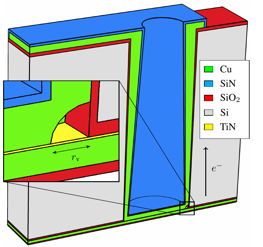
3D integration is an emerging technology which enables highly integrated and complex systems by vertically stacking and connecting various materials, technologies, and functional components together. For the realization of modern 3D ICs new interconnect structures such as through-silicon-vias (TSVs) and solder bumps (SBs), together with complex multi-level 3D interconnect structures, are gaining importance (Fig. 3).
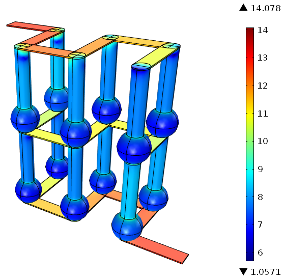
The application of new structures and materials inevitably introduces new reliability issues. The reliability of TSVs and SBs is affected by degradation processes induced by electromigration (EM) and mechanical stresses.
In order to assess the EM reliability and estimate the lifetime of the interconnect, engineers perform tests on specially built interconnect structures under predefined test conditions and calculations based on numerical models.
The development of EM induced voids, eventually leading to interconnect failure, goes through two distinct phases. The first phase is the vacancy diffusion or void nucleation (initiation) phase in which no EM-generated voids are present, and no significant resistance change is observed. The second phase starts after the nucleation of a void and is characterized by void growth, eventually leading to an open circuit failure. Therefore, modeling must be able to address both phases: the behavior of the system prior to void nucleation as well as void evolution and dynamics.
The modeling of the void evolution phase is particularly challenging since it demands mathematical description of the evolving void surface driven by EM, surface diffusion, and gradient of mechanical stress.
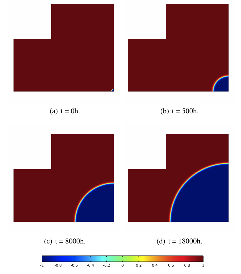
In Fig. 4 the location of the intrinsic void in an Open TSV structure, determined by a simulation of the void nucleating phase, is indicated. Subsequently, void growth is simulated in detail (Fig. 5) by applying the Diffuse Interface approach. Simulations of the void growth mechanism allows for a prediction of the resistance change prior to inevitable EM failure and an estimation of the TSVs lifetime. Similar studies are preformed in order to asses SB reliability.