
 |
|
||||
BiographyYoanlys Hernández Barrios received the bachelor’s degree from Exact Sciences Pre-University Vocational Institute, Pinar del Río, Cuba. He studied Biomedical engineering at the “CUJAE” Technical University in La Habana, Cuba. In August 2015, he began his Master studies focusing on Solid State Electronics at the Center for Research and Advanced Studies of the National Polytechnic Institute (CINVESTAV-IPN) in Mexico City. In August 2020, Yoanlys finished his PhD studies at the same research center specializing in characterization, simulation, fabrication and modeling of thin film transistors and circuits based on amorphous metal oxides semiconductors. In March 2021 he joined the Institute for Microelectronics as post-doctoral researcher and will focus on semiconductor devices and circuits reliability. |
|||||
Impact of BTI on the Performance of Power Electronics Based on SiC MOSFETs
The trapping of charge carriers at the defect densities observed for SiC technology gives rise to a notable time-dependent drift of the transistor threshold voltage known as bias temperature instability (BTI). Based on the results of investigating reliability issues at the transistor level, one can evaluate their impact on the performance of circuits and applications. While computer simulations using physics-based TCAD software are primarily used to explain the characteristics of devices, circuit simulations are often carried out using SPICE software. SPICE simulations are vital for optimizing circuit performance and verifying the stable operation of designs under various operating conditions. In such simulations, compact and physical models which capture the degradation of the devices are required to mimic the behavior of the devices. Typically, compact models based on closed-form mathematical expressions are used for circuit analysis. Such models, however, are usually not very accurate. To ensure full accuracy in simulations, physical charge trapping models — for instance, the two-state defect model — should preferably be used. This model is implemented in our open-source reliability simulator, Comphy.
Our BTI reliability simulator, Comphy, employs a two-state defect model based on the non-radiative multiphonon (NMP) theory to calculate the charge capture and emission events at oxide defects (Fig. 1 - top) and explain the time-dependent drift of the transistor threshold voltage (ΔVth). To ensure full accuracy of our simulation framework, the tools are calibrated considering both DC and short-term AC experimental data (Fig. 1 - center). Using our theoretical model, we can replicate the device behavior for static and quasi-static operation conditions (Fig. 1 - bottom). This now enables us to evaluate more thoroughly the impact of BTI on different circuits. We focused on integrating the extracted data from the physical reliability simulator Comphy into SPICE simulations to evaluate and analyze the impact of the different degradation phenomena over time, as BTI, on circuit applications based on SiC technology. To consider the impact of BTI on the transistors using SPICE simulations, we have to extend the model by adding an independent voltage source to the gate terminal of the transistors. This additional voltage source accounts for the ΔVth, and the schematic of the modified model is depicted in Fig. 2.
In Fig. 3, the simulation process flow using the open-source Ngspice simulator is illustrated. To perform our reliability simulations, we define the net-list of the circuit based on the SPICE model of the SiC MOSFETs (step 1). Next, an external file containing the ΔVth values extracted from Comphy (step 2) for a long operation time (ten years) is used to modify the initial net-list of the circuit. Then we extract the aged parameters of the circuit for a specific degradation and time point, taking into account the principle shown in Fig. 3 (step 3). The Ngspice simulator launches a new simulation every time the initial net-list is modified. However, this net-list modification does not significantly increase the simulation time. As a result of the circuit simulations, we can obtain the aged circuit parameters for long operating time considering the impact of BTI on the SiC MOSFETs. From the simulation data we can extract, for instance, the increase of the propagation delay time of inverter circuits over time [Fig.3 (step 4)].
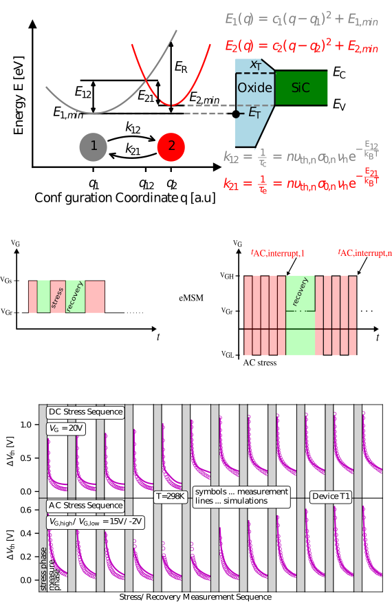
Fig. 1: Schematic of the potential energy surfaces of our physical defect model and the corresponding model parameters required to calculate the charge trapping at defects. (top) The model is based on non-radiative multi-phonon (NMP) theory to calculate the transition times at single defects corresponding to charge transfer reactions. The ΔVth values are extracted considering two different measure-stress-measure (MSM) schemes: a DC PBTI long-term MSM scheme where a constant stress bias is applied before the recovery phase is recorded, and an AC short-term MSM scheme where the ΔVth is measured at different time points tAC, interrupt at which the AC stress signal is interrupted (center-right). The simulations nicely reproduce the measured data set for the ΔVth extracted values of a commercially available SiC power MOSFET (bottom).
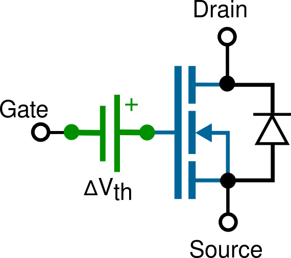
Fig. 2: The BTI impact on the transistors is represented by adding a voltage source with a value equal to ΔVth to the gate terminal of the device. This is considered to modify the subcircuit model of the SiC MOSFET implemented in the Ngspice simulator net-list. ΔVth values are extracted from the accurate physical defect trapping model.

Fig. 3: Simulation process flow using open-source simulator Ngspice, to analyze the BTI impact on the inverter circuits performance. The SPICE simulator uses the data from the reliability simulator Comphy (step 2) to modify the initial net-list of the circuit (step 3). It launches simulations to extract the aged circuit parameters for long operating time. Each simulation corresponds to an inevitable degradation of the transistors for a specific time. With the obtained simulation data we can obtain the aged electrical behavior of the device and circuit parameters — for instance, the propagation delay time of inverters circuits (step 4).