
 |
|
||||
BiographyHans Kosina received the Diplomingenieur degree in electrical engineering and PhD from the Technische Universität Wien in 1987 and 1992, respectively. He was with the Institute of Flexible Automation at the Technische Universität Wien for one year and then joined the Institute for Microelectronics, where he is currently an associate professor. He received the venia docendi in microelectronics in 1998. In the summer of 1993, he was a visiting scientist at Motorola Inc., Austin, Texas, and in the summer of 1999, a visiting scientist at Intel Corp., Santa Clara, California. Dr. Kosina was chairman of the ''11th International Workshop on Computational Electronics'' held in Vienna in May 2006 and is a member of the advisory board of the International Workshop on Computational Nanotechnology. He has served as an Associate Editor of the IEEE Transactions on Computer-Aided Design of Circuits and Systems and the Journal of Computational Electronics. His current research interests include nanoelectronic device modeling and the development of numerical methods and algorithms for classical and quantum transport calculations. |
|||||
Numerical Modeling of Nanostructured Semiconductor Devices
A project on physics-based mobility modeling in strained silicon has been completed. The goal was to predict the piezoresistance coefficients of p-type silicon for a wide range of doping concentrations and temperatures. The empirical pseudo-potential method was used to calculate the electronic band structure of strained silicon, and a full-band Monte Carlo code to calculate the low-field mobility of holes. From the results for various uniaxial stress configurations, the linear piezoresistance coefficients were extracted, and the range of validity and non-linearity effects were estimated.
A project on numerical methods for the stationary Wigner equation and the von Neumann equation has continued. When the von Neumann equation is formulated in rotated coordinates, it turns out that the treatment of the boundaries in the difference coordinate are crucial. A natural way to incorporate double homogeneous boundary conditions is to introduce an absorbing potential layer. This has the effect of damping down the solution near the non-spatial boundaries. We have introduced an alternative formulation based on a symmetric treatment of the spatial and non-spatial coordinates. We apply inflow boundary conditions also at the non-spatial boundaries and require the net inflow to be zero. The developed numerical schemes have been implemented and tested. Both schemes closely reproduce results from the quantum transmitting boundary method. This work demonstrates the numerical robustness of open boundary conditions for the Wigner and the characteristic von Neumann equation.
A project dealing with quantum transport models for device TCAD has continued. A thorough review of the available options regarding quantum transport models has been conducted. These options include the density matrix method, the Pauli master equation, the Wigner equation, and low-order NEGF approximations. Criteria considered were the expected computation time requirements, memory requirements, numerical stability, physical accuracy, and suitability for the target applications. Also the levels of approximation in the band structure models and the scattering models played an important role. To further assess the suitability of NEGF for realistic applications, implementation of a 1D mode space approach in the GTS Nano Device Simulator has commenced.
A Newton-solver that calculates the transverse modes in TMD nanoribbons has been further developed. TMDs in the 1T' phase which are topological insulators were considered. The secular equation resulting from the boundary conditions allows both physical and spurious solutions. A method to uniquely identify the spurious solutions has been developed. Fig. 1 presents the residuum of the secular equation, and Fig. 2 the sub-bands obtained using the Newton-solver.
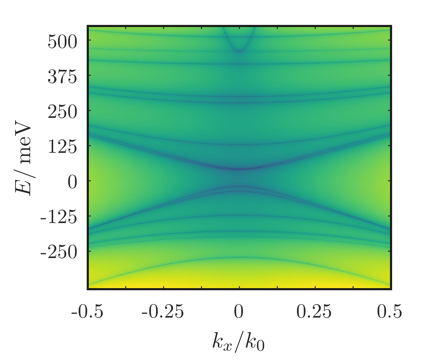
Fig. 1: Residuum of the secular equation for a 28.86 nm wide MoS2 nanoribbon.
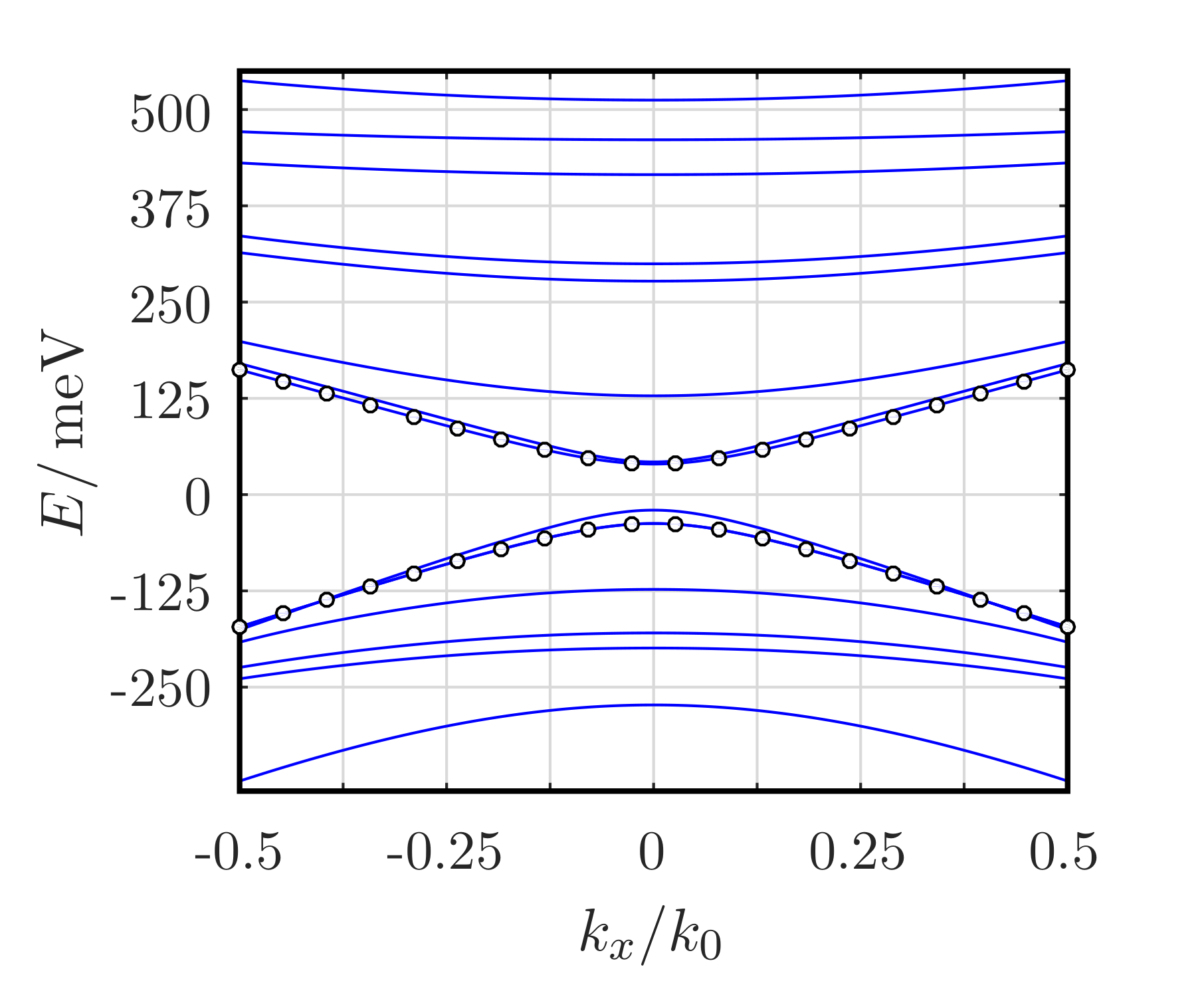
Fig. 2: The root locus of the residuum gives the sub-band structure of the nanoribbon. The two sub-bands marked with circles are spurious ones, and are not part of the physical sub-band structure.