
 |
|
||||
BiographyBibhas Manna was born in Kolkata, India, in 1989. He completed his Bachelor's degree in Electronics and Communication Engineering from the West Bengal University of Technology, India (B.Tech, 2011). He subsequently received his Master's degree in VLSI Design and Microelectronics Technology from the Jadavpur University, India (M.Tech, 2014). He then moved to the Indian Institute of Technology Kharagpur to earn his Doctoral degree in computational nanoelectronics and sensors based on 2D materials (Ph.D., 2021). He joined the Institute for Microelectronics in February 2022 as a postdoctoral research scholar. His current research activities include ab-initio simulation-based exploration of suitable gate dielectrics (e.g., CaF2) for ultra-scaled transistors. |
|||||
DFT-based Atomistic Modeling of CaF2 as a Gate Insulator for 2D Transistors
The trend of continuous miniaturization of field-effect-transistors (FET) to uphold Moore’s law has encountered severe challenges in the deep nanometer regime for silicon channel-based devices due to degraded device performances. This has led to the exploration of various two-dimensional (2D) semiconducting materials to overcome the limitations of standard Si technology and allow further device miniaturization, even down to sub-nanometer channel length. Among them, MoS2 has emerged as the most promising channel material for providing a high-drive current and a reasonable on-off current ratio of the transistor. However, the 2D material still lacks the compatible gate insulator, which could deliver much-improved device characteristics. The ideal gate insulator should have high scalability, a high-quality van-der Waals interface with 2D channel material, reduced trap charges, a high break-down field, and significantly lower vertical tunnel current. Unfortunately, no insulator was reported to possess all these properties simultaneously. The crystalline calcium fluoride (CaF2) has recently gained tremendous interest from researchers as a potential gate insulator for the MoS2 FET due to its ultra-wide bandgap (12.1 eV), ability to maintain quasi van der Waals interface, greater dielectric constant, lesser monolayer thickness, low defect density, etc. Therefore, an in-depth investigation of the structural and electronic properties of CaF2 is of prime importance for attaining optimized device performance. We plan to examine the defects in CaF2 and their influence on device performance. We also want to extend our efforts in computing the tunneling current through the ultra-thin CaF2 layers, which will effectively contribute to transistor leakage currents.
We focus on studying the density functional theory (DFT) based atomistic simulation of various native point defects in CaF2 bulk and surface structures. The point defects are readily introduced into the crystal during the growth process at high temperatures and in complex chemical environments. Such point defects in the gate insulator might cause serious reliability issues to the transistor operating under a higher applied gate field. Thus, an accurate understanding of the point defects in CaF2 and their charge trapping phenomena is essential in designing a highly reliable MoS2 transistor. Typical single point defects in CaF2 are F-center, F interstitial, Ca vacancy, and Ca interstitial. Our preliminary results indicate that the F-center, among all these defects, has a predominant effect on the electronic properties of the insulator. The F-center typically introduces a localized electron trap level at 2.61 eV below the dielectric conduction band minima (CBM). However, the position of the trap is quite far away from the conduction band edge of the MoS2, suggesting a significantly lower affinity toward the gate field-dependent trapping and release of electrons from and to the channel, respectively, as compared to that of the Si-SiO2 case. Other possible point defects in CaF2 also need to be investigated for a meaningful performance evaluation.
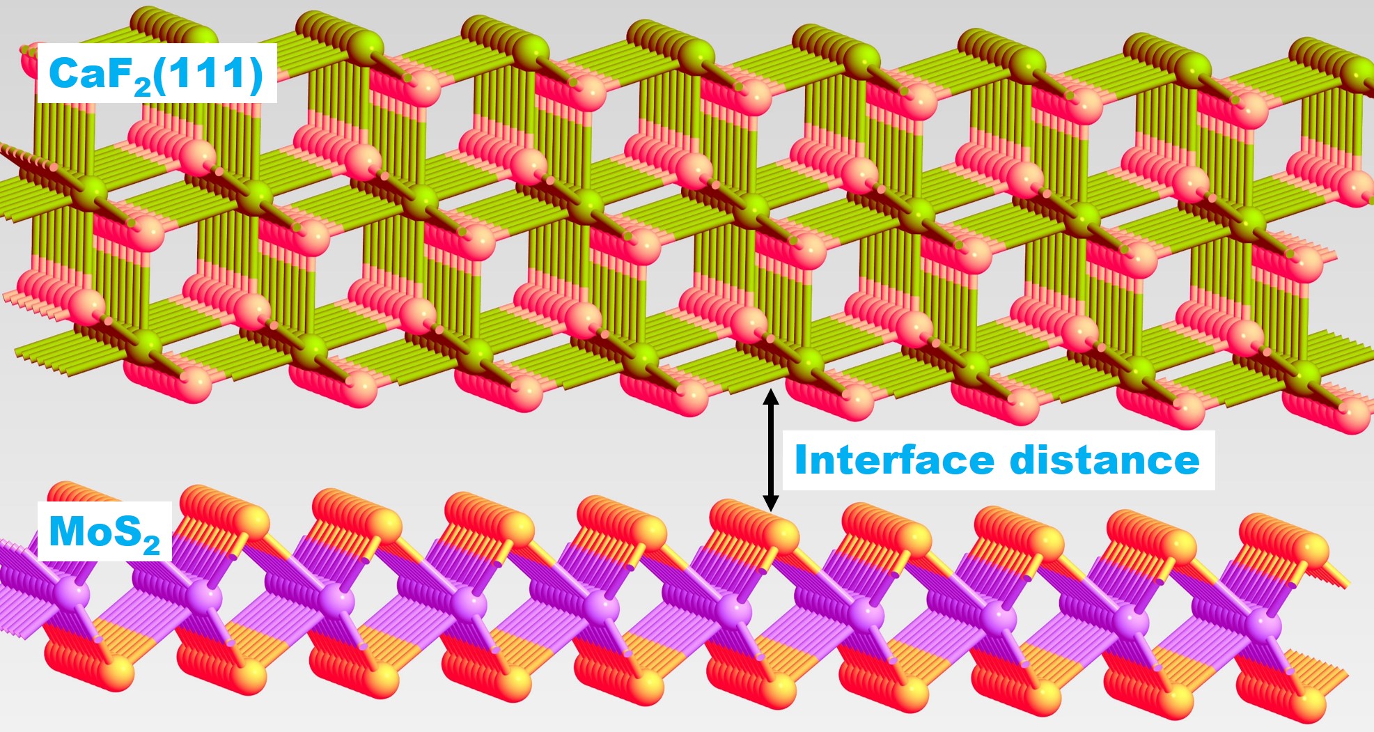
Fig. 1: A schematic showing the quasi van der Waals interface between CaF2(111) gate insulator and MoS2 channel material of a typical 2D transistor.