
 |
|
||||
BiographyJakob Michl was born in Freistadt, Austria, in 1993. He received his MSc degree in Physics from the University of Vienna in 2018. He joined the Institute for Microelectronics in January 2019, where he is currently working on his doctoral degree. |
|||||
Device Reliability at Cryogenic Temperatures
CMOS technologies operating at cryogenic temperatures, i.e., cryo-CMOS, play a key role in the successful deployment of quantum computers. Cryo-CMOS is needed as an electronic control interface operating at 4.2 K to control qubits in the mK-regime. The next key step will be the production of monolithic qubits based on CMOS technology, which should work at low cryogenic temperatures. For this, it is necessary to fully understand the temperature dependence of the MOSFET characteristics. Typically, cryo-CMOS applications are susceptible to noise, such as random telegraph noise (RTN). Therefore, our research has paid special attention to the device characterization and the impact of intrinsic noise at cryogenic temperatures.
One main source of noise is defects in the insulator, or at the interface between the insulator and the substrate. These defects can be introduced during device fabrication or created during operation, and can capture and emit charge carriers from a reservoir, e.g., the conduction/valence band of the substrate or the gate. Many charge capture and emission events simultaneously lead to the well-known 1/f noise characteristics when large-area devices are considered. On scaled devices, single capture/emission can be characterized as discrete steps in the drain-source voltage, and is called RTN.
Charge kinetics can be described using the non-radiative multiphonon (NMP) theory. The neutral and charged defect configuration can be modeled by representing them as potential energy surfaces, which can be approximated by one-dimensional harmonic oscillators. Quantum mechanical tunneling between the two harmonic oscillators enables charge transitions even at cryogenic temperatures, which is also referred to as nuclear tunneling in this context.
Due to nuclear tunneling, RTN does not freeze out. Consequently, noise can be an issue even at 4.2 K. We characterized RTN signals on scaled SiON devices between 4.2 K and 50 K, and analyzed the temperature dependence of the transition rates using NMP theory. Using this approach, we have shown that RTN achieves temperature independence at deep cryogenic temperatures. Using our reliability simulator Comphy, we have shown that defects close to the oxide/insulator interface cause RTN, while defects deeper in the oxide mainly cause bias temperature instability.

Fig. 1: The measured drain-source current at 4.2 K on a scaled SiON device shows discrete steps which contribute to oxide/interface defects that can capture/emit charge carriers. This phenomenon is called random telegraph noise (RTN). The step heights are normally distributed, while the capture and emission time follows an exponential distribution.
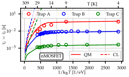
Fig. 2: Three different traps show that the transition rates become temperature independent at deep cryogenic temperatures, which can be modeled using nuclear tunneling.
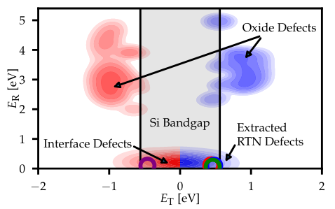
Fig. 3: Using non-radiative multiphonon (NMP) theory and the reliability simulator Comphy, we are able to show that defects close to the oxide/insulator interface are causing RTN, while oxide defects are mainly responsible for BTI.