
 |
|
||||
BiographyAleksandr Vasilev was born in Republic of Mordovia, Russia in 1990. In 2011 he obtained the Bachelor degree in Electronics and Nanoelectronics from Chuvash State University and the Master degree in Solar Heterostructure Photovoltaics at Saint Petersburg Electrotechnical University "LETI" in Russia in 2013. He joined the Institute for Microelectronics in October 2019, where he is working for the FWF project DEMOS and the CDL for SDS. His research focus will be on defect-centric modeling of reliability issues in SiC devices. |
|||||
Modeling the Hysteresis of Capacitance-voltage Characteristics in Lateral 4H-SiC MOSFETs
For over a decade, 4H silicon carbide (4H-SiC) has been used for metal-oxide-semiconductor field-effect transistors (MOSFETs) as a substrate material in power electronic applications. Despite its unique bulk material property, the SiC/SiO2 surface remains an important research topic due to the slightly enhanced defect density compared to SiO2/Si interfaces. To study the interface quality of the MOSFETs, impedance measurements of capacitance-voltage (CV) and conductance-voltage (GV) curves are regularly performed at different frequencies. Their interpretation, however, is not straightforward. This is identified as the stretch-out effect caused by trap charging and discharging during the fast AC signal applied at each gate voltage. Also, CV measurements are sensitive to slow defects in the oxide close to the interface during the up and down sweeps. At each point of the gate, voltage defect states near the Fermi level are charged and retain their charge during the down sweep. These charged defects with slow emission times are responsible for the hysteresis width.
To understand this CV behavior, we have developed TCAD simulations with the Shockley-Read-Hall (SRH) theory for the interface defects and the non-radiative multiphonon (NMP) theory for defects in the oxide and the positive fixed oxide charges. The NMP model was used to calculate the capture and emission times to achieve a more profound understanding of the hysteresis phenomenon. The asymmetry in energy barriers for charge capture and emission processes leads to this effect.
For measurements, we use lateral 4H-SiC nMOSFET with an oxide thickness of 70 nm within the range of −30 V to 30 V at a sweep rate of −4 V/s with a fixed time step.
Our hypothesis about the defect density of states is based on previous research. The fast acceptor-like interface defects are energetically located close to the conduction band and have an exponential distribution. In addition, the slow acceptor-like border traps, with a charge transition level is 0/-1, are energetically located 2.6 eV above the valence band, and have Gaussian distribution. In addition, we use positive fixed bulk oxide charges.
Fig. 1 shows the comparison between measured (symbols) and simulated (lines) CV curves at a temperature of 300 K and a frequency of 256 kHz. To achieve this, we calculated capture and emission times to investigate the effect of the slow border traps on charging dynamics. If emission time at a higher gate bias is slower than down sweep time and capture time, the charges stored at the trap can lead to the hysteresis effect. Also, the fast interface defects have lower capture and emission time and can follow the frequency. In addition, positive bulk oxide defects compensate for the voltage shifts of both types of defects.
Finally, our simulation results nicely explain the hysteresis (see Fig. 1), indicating the high accuracy of our simulation models.
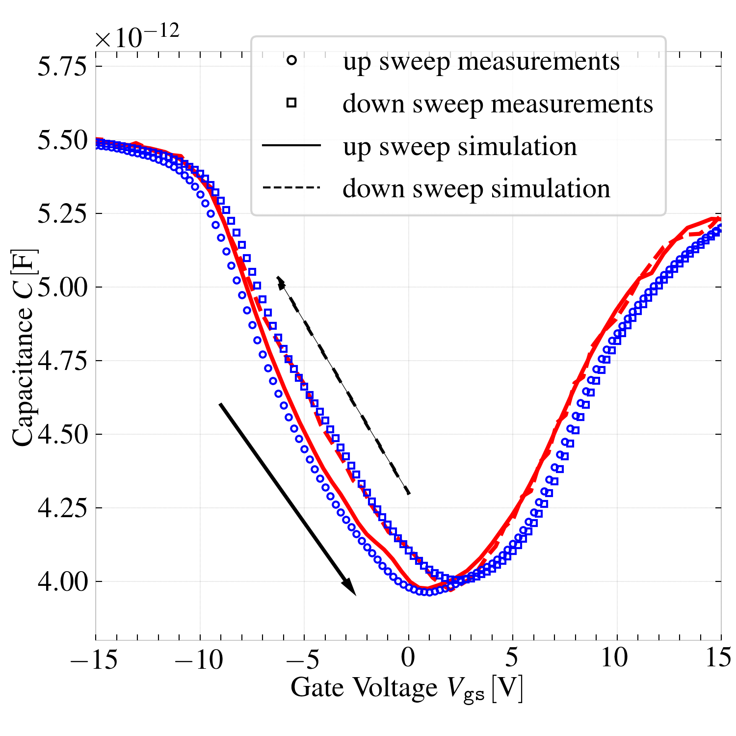
Fig. 1: Measured (symbols) and simulated (lines) CV curves at a temperature of 300 K and a frequency of 256 kHz.