
 |
|
||||
BiographyJosef Weinbub is an Associate Professor of High Performance Simulation in Micro- and Nanoelectronics, an IEEE Senior Member, and a Member of the IEEE Nanotechnology Council's Modeling and Simulation Technical Committee. He obtained the doctoral degree in Computational Microelectronics and the venia docendi (habilitation) in the field of Micro- and Nanoelectronics from the TU Wien. He was a visiting researcher at the EPCC, University of Edinburgh and at the Device Modelling Group, University of Glasgow, Scotland, UK as well as at SILVACO Inc., Santa Clara, CA, USA. He founded and now chairs the master’s program Computational Science and Engineering at the TU Wien and is involved with several international scientific conferences in various management and scientific roles. He is an Associate Editor of the Journal of Computational Electronics and a Principal Investigator of various research projects funded by, e.g., the Austrian Science Fund and the Christian Doppler Research Association. Together with his team he investigates cutting-edge research problems in the area of computational micro- and nanoelectronics. |
|||||
Electron Quantum Optics for Quantum Interference Logic Devices
Electron quantum optics provides the basis for conducting quantum optics-like investigations in a fermionic picture by treating electrons as waves. Compared to quantum optics, solid state electron approaches have the advantage in terms of size, scalability, and the ability of the charge degree of freedom to be easily measurable, with the drawback of a much shorter coherence time. By using numerical simulations based on a Wigner function approach, we show how electron quantum optics principles can be used to realize an electron quantum interference logic device, see Fig. 1. Our design constitutes an alternative for non-magnetic, low-power, and high-performance logic devices allowing for co-integration with conventional electronics. An electron quantum interference logic device is based on injecting individual electron waves into a two-dimensional wave guide which, on the output side, provides three channels. The entire wave guide is sandwiched between two insulating layers, where the top insulator contains two controlling gates which, depending on their biases, allow to change the potential profile affecting the subjacent evolving electron waves. The thus-changeable potential landscape leads to specific interference maxima in the electron density (see Fig. 2 and 3), resulting in different output currents. The emerging current levels enable the definition of logic gates. In particular, universal NAND and NOR gates can be defined. The results show that it is only due to the quantum effects in the transport that these distinct current levels materialize — losing the coherence would result in reduced current level differences, consequently losing stable logic gate definitions. The switching performance of an electron quantum interference logic device entirely depends on the injection performance, e.g., a single-electron source (~10 GHz). The electron quantum interference logic device design shown here provides several directions for adaptations, e.g., number and geometry of the output channels and gates, different wave guide materials, and multi-valued or reconfigurable logic.
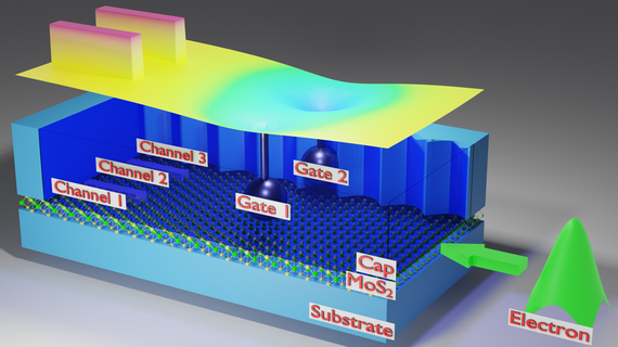
Fig. 1: Schematic representation of an electron quantum interference logic device. An exemplary potential energy distribution of the wave guide is shown on top. The blue cap layer is partially made transparent to show the inside of the device.
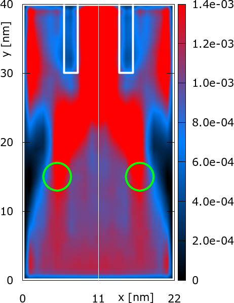
Fig. 2: Distribution of quantum electron density [a.u.] for two symmetric, positive gate bias configurations (green circles). The output channel walls are shown in white.
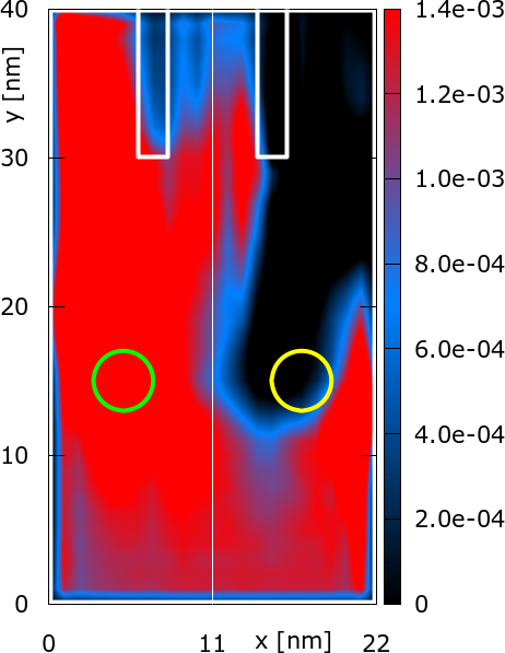
Fig. 3: Distribution of quantum electron density [a.u.] for two asymmetric gate bias configurations (green circle positive, yellow circle negative).