
 |
|
||||
BiographyMauro Borghi was born in 1995 in Reggio Emilia, Italy. He completed his Bachelor's Degree in Mechanical Engineering and Master's Degree in Materials Engineering from the University of Modena and Reggio Emilia. He performed his thesis work at Helmut Schmidt University, Hamburg. He joined the Institute for Microelectronics in 2022, where he is working on the growth and characterization of fluorides for 2D nanoelectronics in collaboration with the University of Modena and Reggio Emilia. |
|||||
Molecular Beam Epitaxy Growth of SrF2 on Ag (111)
The goal of making processors faster and more efficient can be achieved by reducing the size of the transistors, thus fitting more of them onto a microchip. Moore’s law observes that the number of transistors in an integrated circuit doubles almost every two years. While this is still valid today, the continued device scaling using silicon technology is approaching its physical limit. To continue the miniaturization process, new transistor materials are required. One promising innovation lies in the development of devices based on two-dimensional (2D) materials which, however, suffer from a lack of scalable insulators.
Nowadays, silicon technology is most widely used in microelectronics and amorphous bulk oxides are the most commonly applied insulators. However, when moving to low-dimensional devices, oxides which are already known from silicon technology, when grown in thin layers, remain in their amorphous form. This results in many dangling bonds at the channel/insulator interface, which corresponds to many defects, causing charge trapping and accelerated device degradation. Many different insulators have been investigated recently, for their compatibility with various 2D materials, and fluorides have shown to be quite promising. It is also clear that further miniaturization of these devices will require the controlled formation of insulator interfaces directly on metal electrodes, such as the formation of strontium fluoride (SrF2) on the silver (111) surface.
The growth method used to obtain these films is molecular beam epitaxy (MBE) which is a sophisticated form of vacuum evaporation, allowing for the growth of epitaxial films. The term epitaxy indicates the growth of a thin crystalline layer on a likewise crystalline substrate, e.g., Ag (111). The lattice orientation of the film depends on the substrate structure. To achieve this, the solid material of the film (e.g., SrF2) is brought into the vapor phase in a Knudsen cell by heating and the vapor condenses on top of the substrate. This process takes place in an ultra-high vacuum (UHV) chamber at a base pressure of 2.0×10⁻¹⁰ mbar, in order to avoid as many unwanted impurities as possible and to increase the mean free path of the molecules in the chamber. Epitaxy is achieved if the lattice mismatch between the two crystalline materials is low. The lattice mismatch of SrF2 (lattice parameter 0.580 nm) and silver (lattice parameter 0.409 nm) is around 5 %, when considering the differences between three metal atom spacings and two fluoride cation spacings (see Fig. 1). The outermost surface is F-terminated, guaranteeing sharp and almost ideal Van der Waals interfaces, which is essential to ensure sufficiently high performance of future 2D devices.
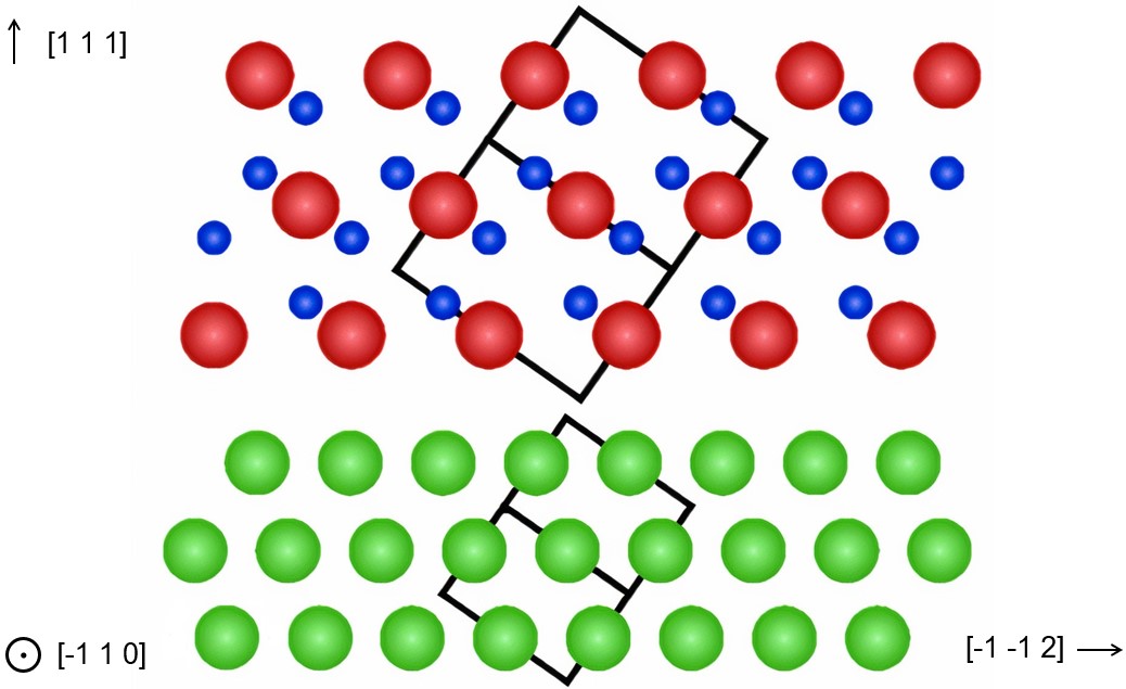
Fig. 1: Illustration of the interface between the silver (green atoms) and the strontium fluoride film (red atoms correspond to the strontium and blue atoms represent fluorine).