
 |
|
||||
BiographyMohammad Davoudi received his bachelor's in Atomic and Molecular Physics from the Iran University of Science and Technology. He then started his master's in Particle Physics at Shahid Beheshti University where his research focused on Entanglement Entropy, Quantum Chromodynamics, and Gauge/Gravity duality (AdS/CFT). After graduation in 2019, he taught physics as a lecturer at the University of Eyvanakey. In June 2022 he joined the Institute for Microelectronics, working on novel semiconductors and insulators for the next generation of electronic devices, specifically FET transistors. |
|||||
Exploring Bi2SeO5 as a Promising Gate Insulator for 2D Semiconductor-Based Field-Effect Transistors
As the demand for faster and smaller transistors continues to grow for advanced semiconductor technology nodes, the inherent complexity of the system architecture likewise increases on all levels. This demand has pushed leading semiconductor manufacturers to explore new potential solutions, including the use of stacked nanosheet field-effect transistor (FET) designs. However, despite their promise, these nanosheet devices still have limitations in channel thickness, when further scaling is required, which has prompted the need to investigate alternative materials.
Fortunately, two-dimensional (2D) semiconductors have shown promising results in maintaining sizable mobilities at atomic-layer thicknesses below one nanometer. However, the development of 2D semiconductor-based FETs still poses several challenges, one of which is identifying suitable gate insulators which can provide a high-quality interface, a small concentration of electrically active border traps, and further scalability to small insulator thicknesses.
One of the most promising candidates for a gate insulator for 2D-based FETs is Bi2SeO5. Bi2SeO5 is known for its high-k and high mobility, and it can be fabricated with a smooth interface through the oxidization of Bi2O2Se. Despite its promise, further research is still required to determine and realize the full potential of Bi2SeO5 and other 2D materials.
To model hysteresis in the transfer characteristics of a FET, device modeling and the simulations of the device (see Fig. 1) under operating conditions are performed using the drift diffusion equation and the non-radiative multi-phonon model (see Fig. 2) to describe charge capture and emission at charge traps in the insulator. These simulations aim to accurately model the behavior of the FETs and to identify potential reliability issues which may arise.
In conclusion, the search for suitable gate insulators for 2D nanoelectronics is a critical ongoing research effort which could lead to significant advancements in the semiconductor industry. SiO2 has high interface trap densities and charge trapping events, making it an inadequate option. However, promising candidates like Bi2SeO5 and other 2D materials are being explored, and further research and development are needed to unlock their full potential.
Overall, the field of microelectronic research into novel transistor designs is an exciting one, with numerous possibilities for the future. However, there is still much work to be done to address the challenges which arise as semiconductor technology advances.
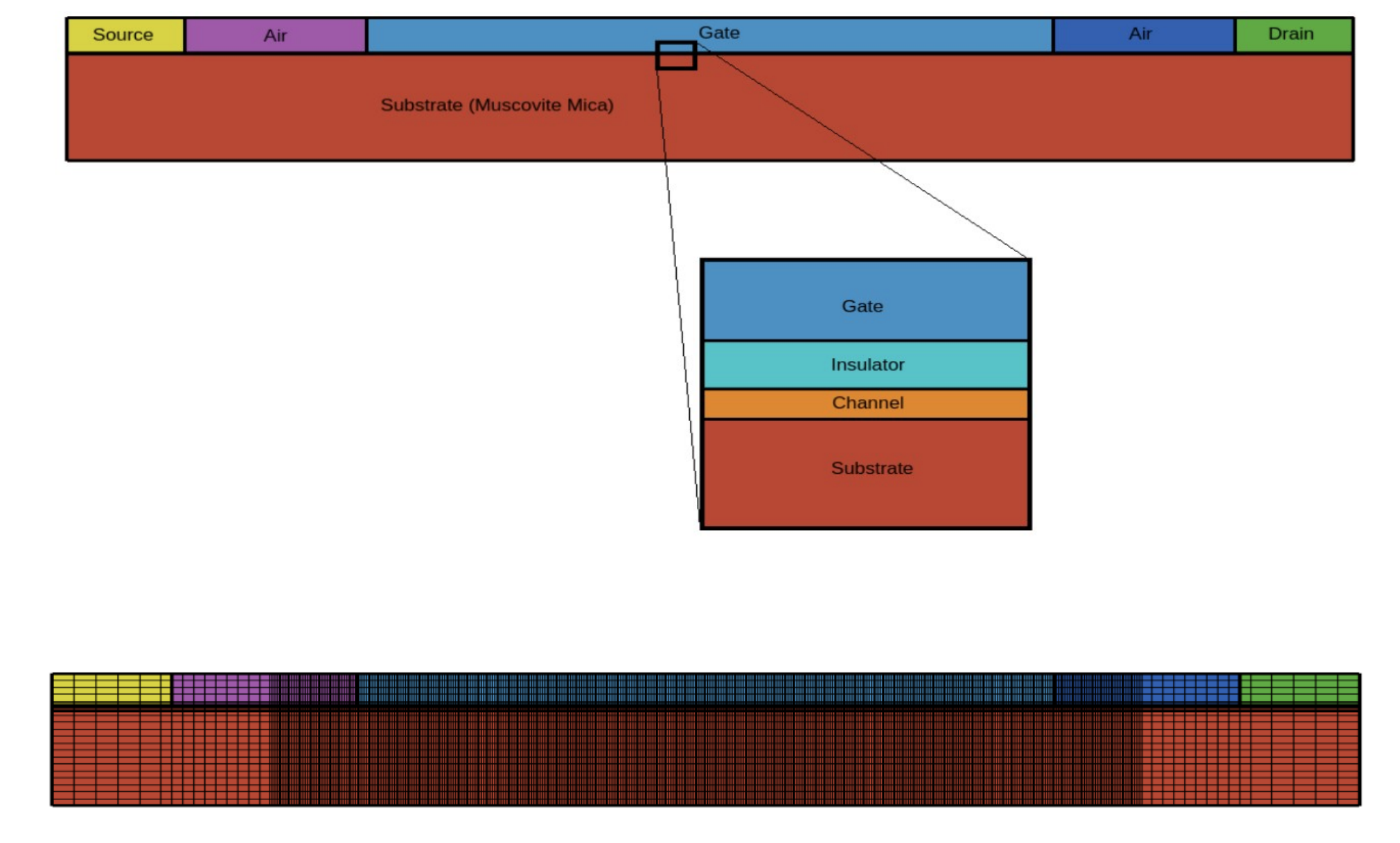
Fig. 1: Geometry of the device under simulation.
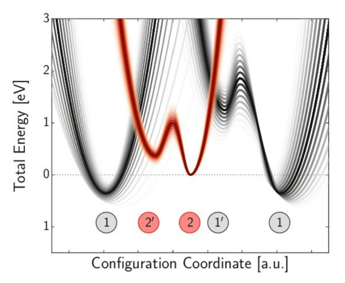
Fig. 2: Non-radiative multi-phonon model.