
 |
|
||||
BiographyAlexander Karl rreceived his Bachelor and Master degrees in Technical Physics from TU Wien in 2020 and 2022, respectively. For his Master's thesis he focused on the search for Dark Matter with the CRESST experiment. In August 2022 he joined the Institute of Microelectronics and is pursuing his PhD studies. Currently, his research is focused on the modeling of 2D field effect transistors using, e.g., the compact physics framework Comphy, and on investigating the application of novel 2D materials towards the realization of electronic devices. |
|||||
Comphy – A Compact Physics Framework for the Simulation of Reliability Issues in 2D Nanoelectronics.
To improve the performance of electronic devices, the number of transistors in integrated circuits has been increased steadily in recent decades. It used to be a rule of thumb, typically termed Moore's law, that the number of transistors in an integrated circuit (IC) doubled about every two years due to the shrinking size of transistors. However, the miniaturization of conventional silicon MOSFETs is gradually reaching its physical limits since some physical properties, such as mobility, degrade drastically as soon as the layer thickness falls below a few nanometers. Two-dimensional (2D) semiconductors appear to be a promising alternative, since certain 2D materials have favorable electronic properties despite their atomic-layer thicknesses.
Regardless of the immense interest and abundant research output in 2D materials, it is still unclear which 2D semiconductors have the potential to compete with conventional silicon technology which has been optimized over the past six decades. One of the central research questions is which combination of 2D semiconductor channel and insulator exhibits a high-quality interface with a low density of electrically active defects, thereby leading to transistors with an improved reliability.
To help answer the above question, the Python framework Comphy was extended by a compact model describing the electrostatics of 2D transistors. The semiconductor in 2D MOSFETs acts as a quantum well (see Fig. 1), which leads to a constant density of states in the conduction/valence band of the semiconductor and thus to significant differences in the electrostatics of the device, compared to conventional three-dimensional (3D) or bulk devices.
In the next step, the framework is extended with the possibility of adding defects to the device, as shown in Fig. 1. The defects are modeled using an effective 2-state non-radiative multiphonon (NMP) model, which has already been used successfully to describe defects in 3D devices. This extension of the framework will make it possible to simulate charge trapping phenomena in 2D MOSFETs, which, in turn, will allow to extract defect parameters from hysteresis and bias temperature instability (BTI) measurements in order to identify physical defect candidates.
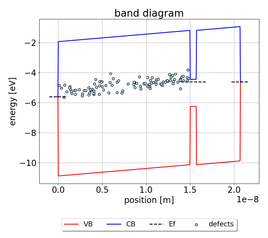
Fig. 1: Band diagram created with the implemented compact model for double gated 2D MOSFETs. The corresponding device consists of a MOS2 layer stacked between two SiO2 layers. The blue (red) curve shows the conduction (valence) band of the gate stack.