
 |
|
||||
BiographyPedram Khakbaz was born in Arak, Iran. He received his Ph.D. degree in electronics engineering from the University of Udine, Italy, in 2022 where he studied the electronic transport in devices based on two-dimensional semiconductors. From Sep. 2016 to Sep. 2018, he was with the computational nano-electronics lab and finished his M.Sc. degree in nano and micro-electronics engineering at the University of Tehran, Iran. In June 2022, Pedram joined the Institute for Microelectronics as a postdoctoral researcher and his current research interests include ab initio modeling and quantum transport for the modelling of devices based on 2D semiconductor materials. |
|||||
DFT Investigation of Insulators for 2D Material Based Nanoelectronics
High-κ dielectrics are essential materials in modern nanoelectronic devices and have attracted substantial attention in recent years. These materials play an important role in regulating the flow of charge carriers in the channel of field-effect transistors (FETs), which are the building blocks of modern electronics. In a FET, the high-κ dielectric acts as an insulating layer between the gate and channel, and its primary function is to sustain a strong electric field at the gate, which controls the flow of charges in the channel and regulates the device’s on/off state. With the growing demand for high-performance and low-power electronics, the use of two-dimensional (2D) materials in nanoelectronics is gaining increasing attention. 2D materials, such as graphene and transition metal dichalcogenides (TMDs), offer several advantages over traditional three-dimensional (3D) materials, including high mobility, atomically thin device channels, and relatively defect-free van der Waals interfaces, making them attractive for use in next-generation ultimately scaled electronic devices. However, the integration of 2D materials in electronic devices is hindered by several challenges, one of them being the lack of high-κ dielectrics with atomically sharp and flat surfaces. For a high-κ dielectric material to be suitable for integration in 2D material-based FETs, it must possess several fundamental properties. Firstly, it should exhibit a high dielectric constant (κ), allowing the application of strong electric fields for small layer thicknesses. Secondly, it must have atomically sharp and flat surfaces, which is critical to minimize scattering at the interface and maintain the theoretically high mobility of the 2D material channel. Finally, the material should exhibit stability and low leakage currents, ensuring high reliability and performance of the 2D FETs. Utilizing density functional theory (DFT), we investigate the structural, optical, and electronic properties of emerging high-κ dielectric candidates for applicability as insulators in two-dimensional field-effect transistors (2D FETs). Among these, bismuth selenite (Bi2O5Se) is of particular interest, as it exhibits two distinct phases, illustrated in Fig. 1.
The high-mobility 2D semiconductor, Bi2O2Se, features a body-centered tetragonal lattice structure, characterized by the I4/mmm space group (number 139) and lattice parameters a=b=3.88 Å and c=12.16 Å. This lattice comprises alternating [Bi2O2] and [Se] layers, representing positive and negative layers, respectively (see Fig. 1). Although stable under ambient conditions, mild oxidation of Bi2O2Se can be achieved through exposure to atomic oxygen, generated via vacuum-ultraviolet (185 nm) photolysis of O2. This process induces intercalative oxidation of the [Se] layers, sequentially unzipping the planar [Bi2O2] frameworks and causing interlayer expansion from 6.1 Å to 7.8 Å. The 2D [Bi2O2] framework remains intact throughout the oxidation process. The resulting single-crystalline native oxide, consisting of [SeO3] anion layers interspersed between [Bi2O2] layers with an interlayer spacing of approximately 7.8 Å along the c-axis, is denoted as β-Bi2O5Se, distinguishing it from the α-Bi2O5Se synthesized through thermal oxidation or powder sintering (see Fig. 1).
Downscaling of field-effect transistors in integrated circuits leads to higher speed, lower power consumption, and increased integration density, but also results in detrimental short-channel effects. Transistors designed using high-mobility 2D semiconducting channels and ultra-thin high-κ dielectrics can suppress these effects by scaling the characteristic length λ. To analyze the thickness dependency of α-Bi2O5Se, the electronic band structure and effective masses have been calculated using DFT for different thicknesses. As shown in Fig. 2, by increasing the thickness, while the effective mass in the y-direction increases, there is a very slight decrease in the bandgap and mx. In addition, by decreasing the physical thickness, the permittivity, εox, also reduces for thicknesses below the bulk value (see Fig. 3). This can be a limit for further reducing the equivalent oxide thickness.
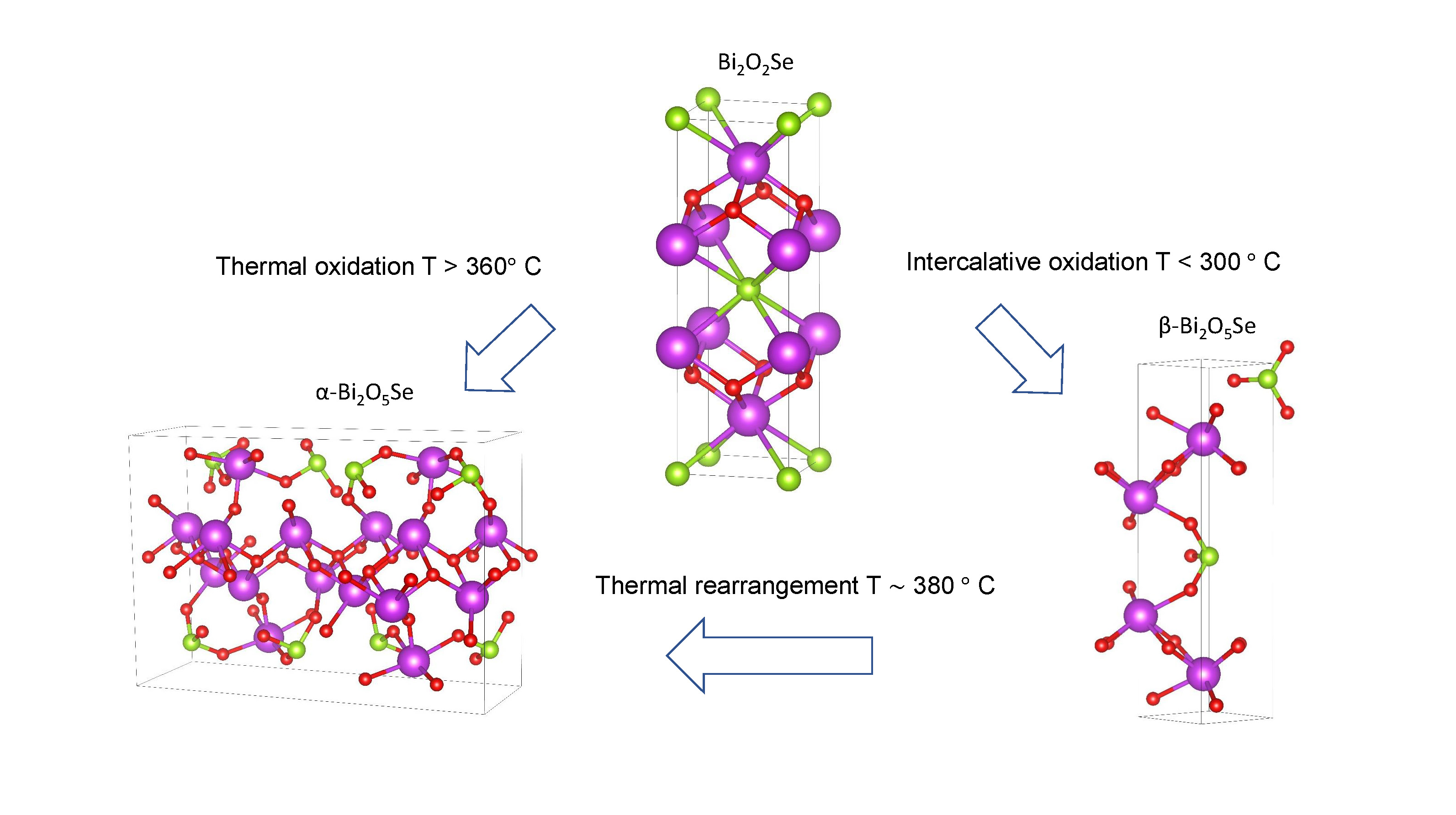
Fig. 1: Crystal structure of Bi2O2Se and its two native oxides.
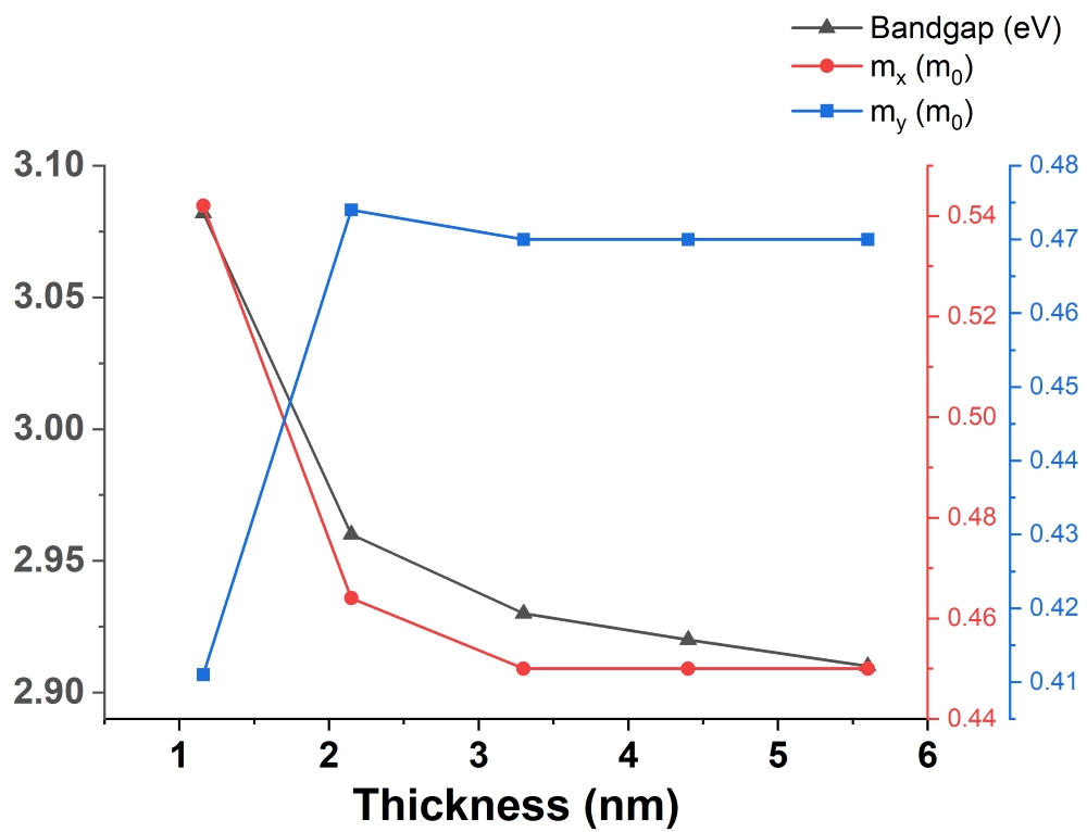
Fig. 2: Bandgap and effective masses (mx and my) as a function of thickness for α-Bi2O5Se. By reducing the thickness, the oxide bandgap and mx increase slightly.
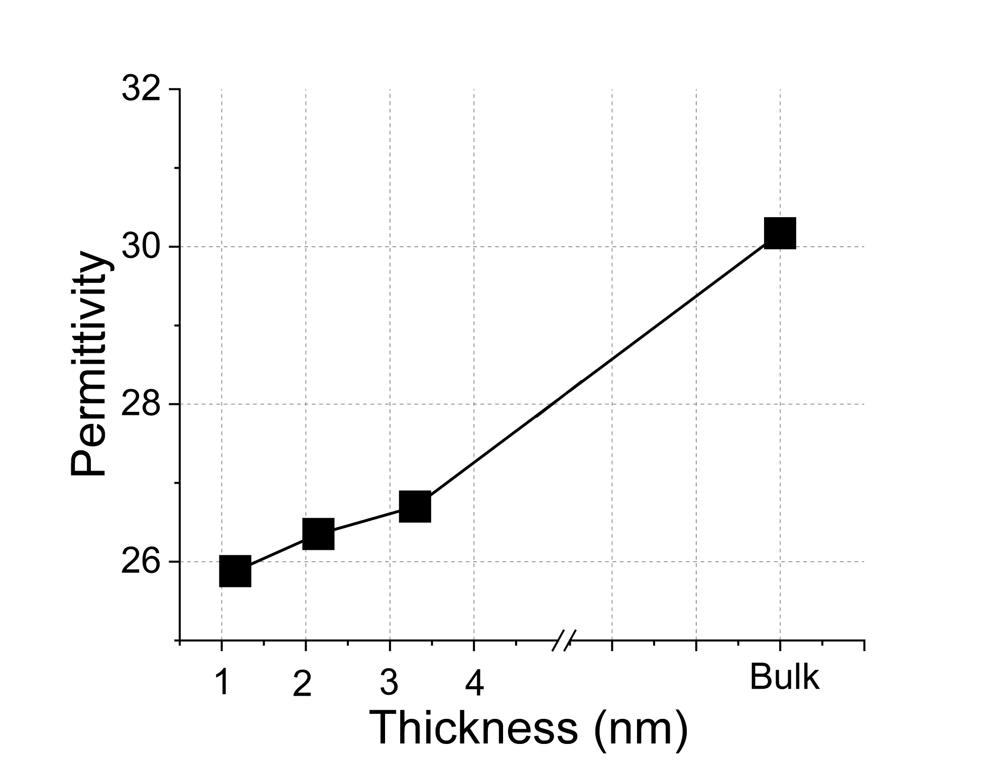
Fig. 3: Calculated permittivity as a function of thickness for α-Bi2O5Se. By reducing the thickness, the oxide permittivity decreases.