
 |
|
||||
BiographySeyedmahdi Sattari-Esfahlan received his Master's degree in Photonics and Nanoelectronics from the University of Tabriz, Iran in 2016 and his Doctorate in Electronic Engineering from the Seoul National University/Gachon University, South Korea in 2022. During his PhD his main research focus was on advanced material science, nanoelectronic devices, and neuromorphic computing. As a postdoctoral fellow, he joined the Institute for Microelectronics at TU Wien in August 2022. Currently, Dr. Sattari-Esfahlan is working on the device fabrication and characterization of 2D-material-based electronic devices with different gate insulators, analyzing the performance and reliability of 2D FETs. |
|||||
Fabrication of 2D-FET Devices with Emerging Gate Insulator Materials and Their Reliability Analysis
Two-dimensional (2D) material-based field-effect transistor (FET) channels demonstrate higher mobilities than their bulk counterparts, which is important for maintaining the scaling criteria of Moore’s law once silicon’s scaling limit is reached. However, the universal properties of the gate insulator and its interface with the channel are the two main components which can significantly degrade the performance of 2D-FET devices. Practically, 2D-FETs mostly suffer from unsuitable subthreshold swings (SS) and lower than theorized carrier mobilities. The degradation of key device parameters is rooted in the properties of the implemented gate insulators. Therefore, the discovery of compatible insulators which can reduce the impact of these negative factors and finally fabricate high-performance 2D-FETs is highly complex. One potential insulator which has demonstrated high promise for integration with 2D semiconductors via van der Waals interactions is strontium titanate SrTiO3 (STO), a high-k oxide with a high dielectric constant of around 300 at room temperature. STO overcomes the charged impurity scattering and has shown to provide higher mobilities in 2D/STO FETs than many other insulators. Another potential gate insulator which has shown positive behavior for 2D FETs, including an exceptionally low density of insulator defects (responsible for hysteresis and long-term drifts of the FET performance) and considerably fewer leakage currents, is nanometer thick CaF2.
Our research aims to fabricate FET devices using various 2D materials as semiconducting channels and implement the above-mentioned gate insulators to overcome the performance limitations of 2D-FET devices. In this regard, transfer characteristics, hysteresis, and bias temperature instability (BTI) of fabricated FET devices are demonstrated. Initial current-voltage (I-V) characteristics and reliability analysis based on a STO/MoS2 FET device are performed. The device demonstrates an ON/OFF current ratio (ION/IOFF) of above 104 within the top-gate voltage range of ±1 V at room temperature. Also, low-temperature analysis at 78 K showed negligible hysteresis. However, at a higher temperature of about 250 K, the hysteresis width reached its peak value. Higher degradation at higher temperatures arises from the thermally activated nature of charge trapping, thereby increasing the hysteresis. Also, the BTI analysis exhibited charging/discharging of the oxide traps within a close vicinity of the interface.
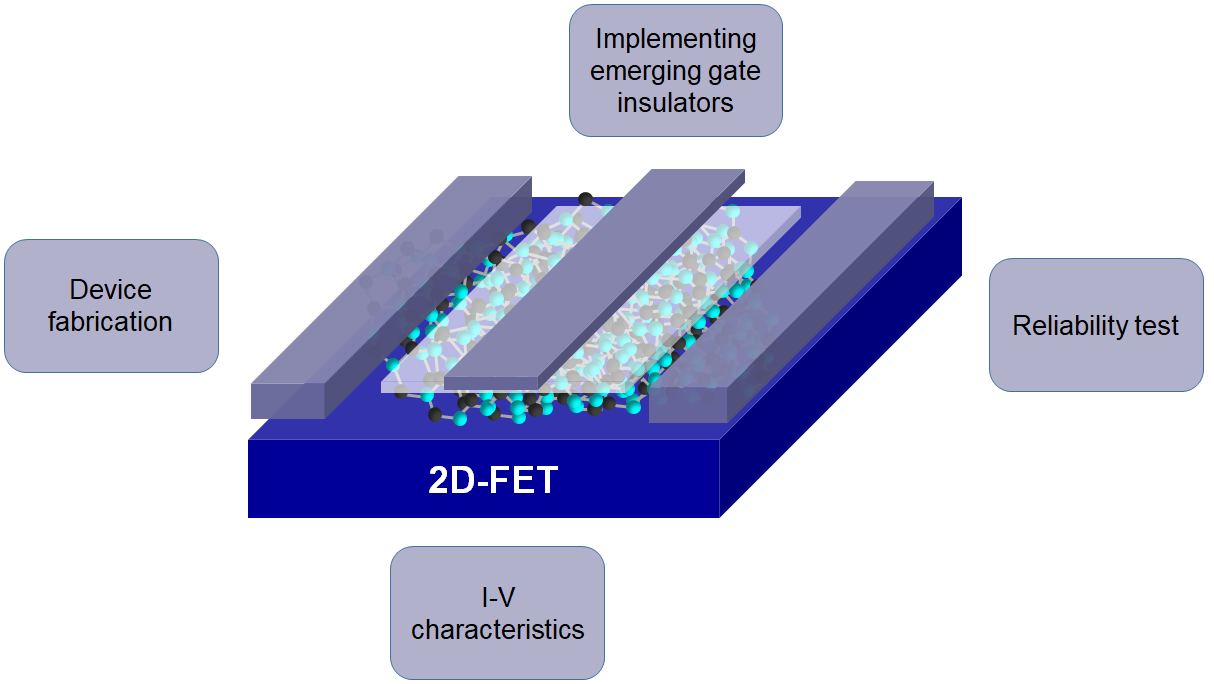
Fig. 1: Research diagram for the fabrication and reliability analysis of a 2D-FET device.