
 |
|
||||
BiographyMate Ćapin was born in Kiel, Germany, and received both his Bachelor and Master’s degrees in physics at Christian-Albrechts-University in Kiel, Germany, in the Computational Solid State Theory group of Fabio Caruso. Mate joined the Institute for Microelectronics in March of 2023, where he is pursuing a PhD degree with a focus on understanding the electrical properties of two-dimensional materials (e.g., MoS2) and their application in digital field effect transistors (FETs) and sensors. |
|||||
Multi-Scale Modeling of Doped MoS₂ for Enhanced Gas Sensing
Two-dimensional Transition Metal Dichalcogenides (TMDs), such as molybdenum disulfide (MoS2), are promising candidates for gas sensing due to their low power consumption and tunable bandgap. These properties allow for sensitivity control via structural modifications, particularly through substitutional and vacancy doping, which can enhance electronic transport and sensing performance.
The focus is set on a computational investigation of doped MoS₂ using a multi-scale approach combining first-principles simulations, transport modeling, and lattice dynamics. Density Functional Theory (DFT) was used to assess how doping and vacancies alter the atomic and electronic structure, enabling targeted tuning of material properties for improved gas sensing.
To reflect experimental conditions more accurately, CP2K simulations explored how atomic substitutions affect local geometry and charge distribution, key factors in determining the material’s electronic transport behavior. Phonopy was employed to analyze phonon dispersion in both pristine and doped MoS₂, offering insight into dynamic stability and the impact of lattice vibrations on carrier mobility and gas interactions.
Further, EPW calculations provided a deeper understanding of electron-phonon interactions, critical for modeling charge transport and scattering mechanisms under realistic conditions. At the device level, QuantumATK was used to simulate current-voltage (IV) characteristics across various geometries and doping setups, highlighting how atomic-scale changes influence current flow. Given the edge-dominated nature of transport in 2D materials, appropriate contacts were modeled to capture realistic behavior.
This integrated computational framework effectively connects atomic-level modifications to device-scale performance, supporting the design of next-generation, high-sensitivity gas sensors based on engineered 2D materials. Each tool was selected for its strengths at a particular scale enabling a comprehensive evaluation of doped MoS2. This integrated approach ensures that insights gained at the quantum level are meaningfully translated into predictions of device performance.
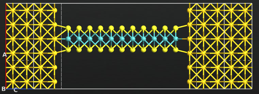
Fig. 1: Edge-contacted MoS₂ device structure modeled in QuantumATK, showing MoS₂ channel connected to gold electrodes.