
 |
|
||||
BiographyNils Petter Jørstad was born in Warsaw, Poland, in 1995. He received his Bachelor’s degree in Physics at the Norwegian University of Science and Technology (NTNU), Norway, in 2019. After a summer internship at Manipal University in Jaipur, India, he enrolled in the Master’s program in Physics at NTNU. He obtained his Master’s degree in 2021, specializing in computational physics. Nils joined the Institute for Microelectronics in September 2021, where he is pursuing a PhD degree focusing on the implementation of spin and magnetization dynamics in simulations of non-volatile magnetic memory devices. |
|||||
Micromagnetic Modeling of Spin-Orbit Effects in Spintronic Devices
Emerging spintronic devices exploit materials with strong spin-orbit coupling (SOC), typically heavy metals (HMs) like tungsten (W), tantalum (Ta), and platinum (Pt), to manipulate the magnetization in adjacent ferromagnetic (FM) layers. The SOC induces the interfacial Dzyaloshinskii-Moriya Interaction (IDMI), an antisymmetric exchange interaction that stabilizes Néel-type domain walls and chiral spin textures, such as skyrmions. When an electric field is applied across the HM, the spin Hall effect (SHE) generates a pure spin current, which is injected into the FM layer. At the HM/FM interface, the SOC, combined with the broken inversion symmetry, creates a spin accumulation via the Rashba-Edelstein effect (REE).The spins polarized transverse to the magnetization quickly dephase and transfer their spin-angular momentum to the magnetization, resulting in a current-induced magnetization torque known as spin-orbit torque (SOT).
SOTs enable efficient, current-driven switching of magnetic states, ideal for applications such as non-volatile magnetoresistive random access memory (MRAM). In MRAM, the logical state is stored in the relative orientation of two FM layers separated by an oxide, forming a magnetic tunneling junction (MTJ). Writing the state typically necessitates high currents through the MTJ, which degrade the oxide barrier and limit the device's endurance. Introducing an HM layer enables SOT-based writing and separate read and write paths, drastically improving the endurance.
To facilitate the development of such devices, there is an increasing demand for fast and accurate simulation frameworks. A promising approach involves coupling spin and charge transport with magnetization dynamics to capture the full behavior of the device. Micromagnetic simulations are particularly effective for exploring nanoscale phenomena like domain wall motion and spin waves. When extended to include spin-orbit effects such as IDMI, SHE, and REE, these simulations can provide valuable insights for advancing next-generation spintronic technologies that utilize spin-orbit coupling (SOC).
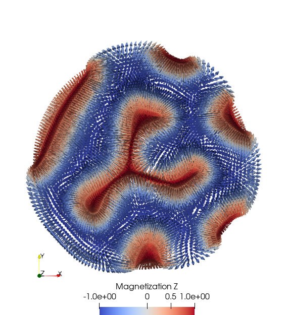
Fig. 1: Multiple magnetic domains forming in a ferromangetic disk with a 80 nm diameter due to a strong interfacial Dzyaloshinskii-Moriya interaction.