
 |
|
||||
BiographyHans Kosina received the Diplomingenieur degree in electrical engineering and PhD from the Technische Universität Wien in 1987 and 1992, respectively. He was with the Institute of Flexible Automation at the Technische Universität Wien for one year and then joined the Institute for Microelectronics, where he is currently an associate professor. He received the venia docendi in microelectronics in 1998. In the summer of 1993, he was a visiting scientist at Motorola Inc., Austin, Texas, and in the summer of 1999, a visiting scientist at Intel Corp., Santa Clara, California. Dr. Kosina was chairman of the ''11th International Workshop on Computational Electronics'' held in Vienna in May 2006 and is a member of the advisory board of the International Workshop on Computational Nanotechnology. He has served as an Associate Editor of the IEEE Transactions on Computer-Aided Design of Circuits and Systems and the Journal of Computational Electronics. His current research interests include nanoelectronic device modeling and the development of numerical methods and algorithms for classical and quantum transport calculations. |
|||||
Device Simulation and Transport
Device simulation is a branch of Technology Computer Aided Design (TCAD) and has become an indispensable tool within the semiconductor industry. Research into future technology nodes requires physics-based device simulation beyond the capabilities of traditional TCAD which was based on the drift-diffusion approximation. Applications of device simulation are manifold, and include strain and band-gap engineering, variability studies, as well as degradation modeling and life-time prediction. Path-finding research into novel materials such as III-V, SiC, and TMD, and novel device concepts require steady advancement of physics-based simulation tools. Especially effects originating from the quantum mechanical nature of charge carriers, such as band structure and transport properties, play an important role, and the development of accurate and yet computationally effective models for new materials and structures is an active research area.
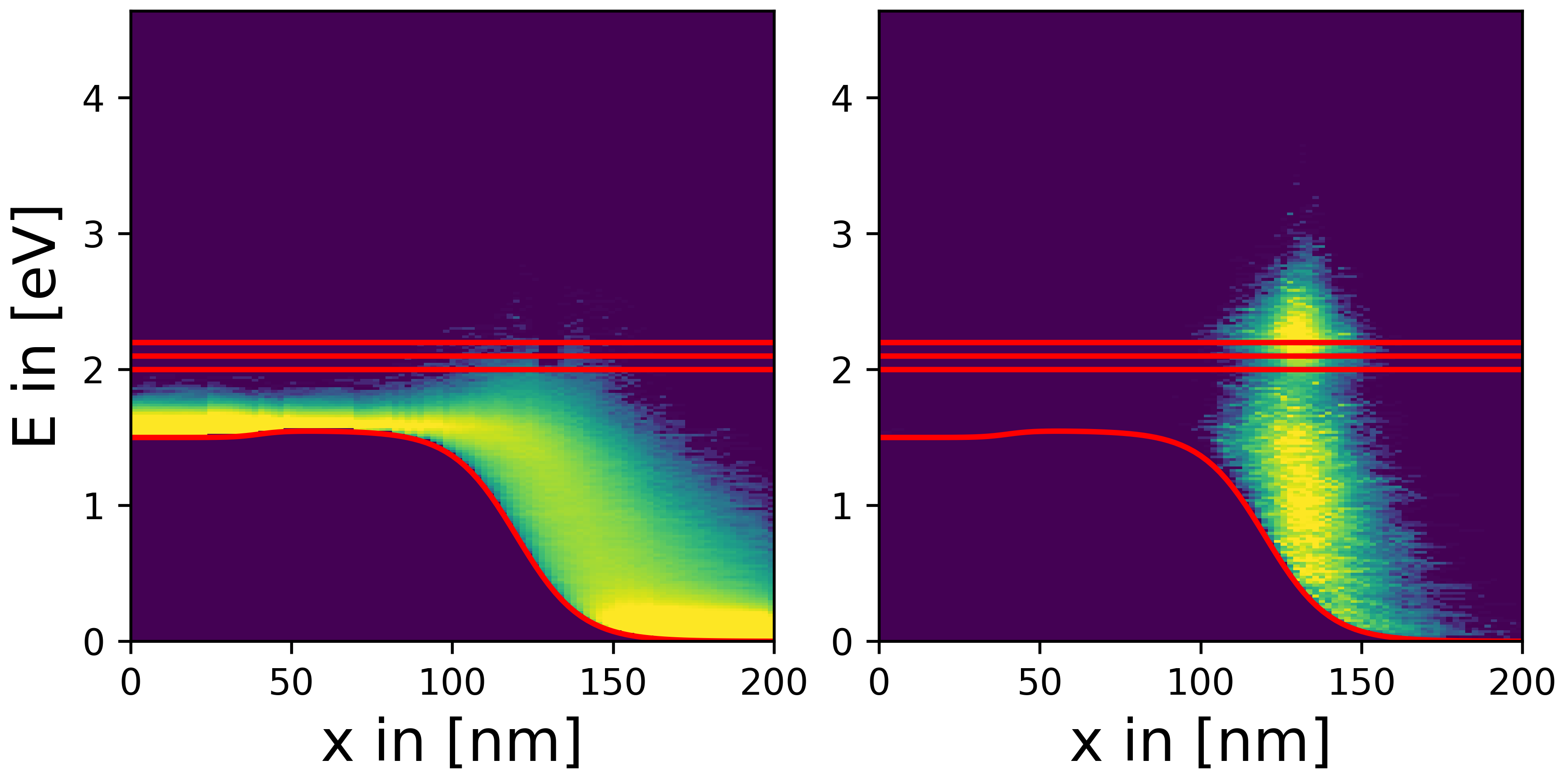
Fig. 1: Distribution of sampling points with large (left) and small (right) statistial weight in a Monte Carlo simulation of a MOSFET inlcuding electron-electron scattering.