
 |
|
||||
BiographyRoman Kostal received his master's degree in Applied Mathematics and Scientific Computing from the University of Vienna in 2023. He joined the Institute for Microelectronics as a doctoral candidate in 2024 where he is working on semiconductor process simulation. His research is focused on predicting topography evolution and geometry generation based on chamber parameters using machine learning approaches. |
|||||
New Parameter Search and Optimization Tools for Process TCAD Model Development
Thin film deposition and etching are essential methods for semiconductor device fabrication. Simulation models of these processes often depend on a collection of parameters specified by the user, typically derived from experimental measurements. To avoid trial-and-error parameter search, the parameters can be systematically adjusted using automated optimization techniques. The goal is to align the simulated outputs with experimental observations and develop models with predictive capabilities. Typically, experimental information is derived from two-dimensional (2D) electron microscopy images. Since reconstructing full three-dimensional (3D) structures is costly and complex, validation efforts are usually confined to comparing 2D feature profiles (FPs). Geometric descriptors (GDs) of the final structure such as film thickness, total etch depth and taper angle are then used to formulate the optimization objective.
We have recently implemented new approaches to several steps of this workflow in our custom simulation platform ViennaPS. First, we developed methods to seamlessly extract 2D slices from 3D simulation domains which can then be compared to experiment, shown in figure 1 left. Second, rather than relying on local, ambiguous, user defined geometric descriptors, we implemented new global metrics for profile comparison, see figure 1 middle and right. These serve as robust objective functions for derivative-free optimizers and lead to excellent optimization performance. Finally, we are using tools for analysis of global sensitivity of the objective function value to the model parameters. This provides key insights into the relative importance of the model parameters and helps with the choice of decision variables for optimization. All in all, these new tools accelerate the development of predictive simulation models of deposition and etching.
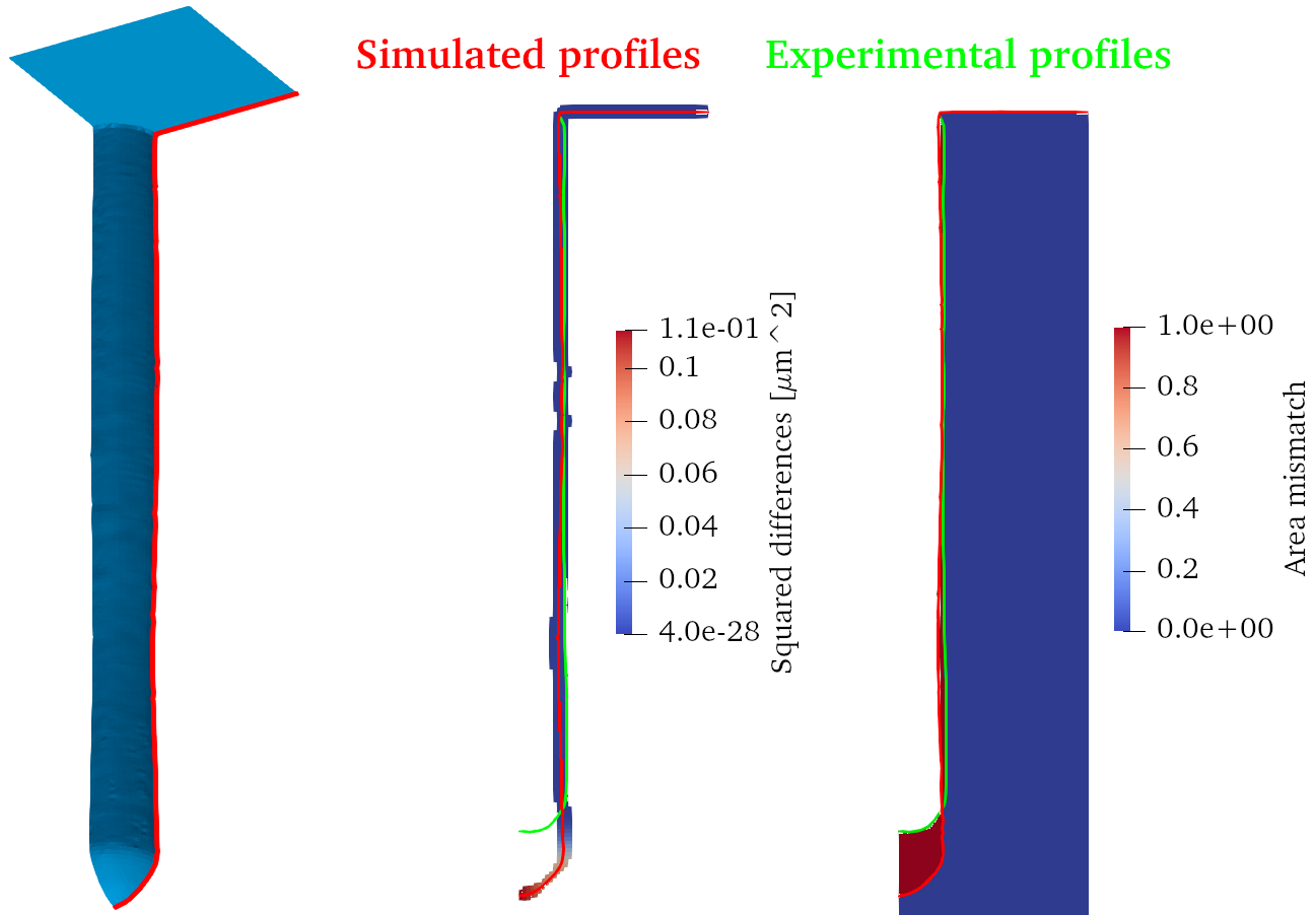
Fig. 1: Illustration of the new tools on the process of Si hole etching in an SF6/O2 plasma. Left: A quarter of a hole was simulated in 3D, the 2D profile was extracted. Middle and right: Comparison of the simulation and experiment using a distance metric and an area mismatch metric, respectively.