
 |
|
||||
BiographyPaul Sommerer was born in Gmunden, Austria, in 1996. He studied Technical Physics at the TU Wien, receiving his BSc degree and Diplomingenier in 2020 and 2024, respectively. In August 2024, he joined the IuE as a PhD student, focusing on designing and evaluating circuits embedded in CMOS image sensors. |
|||||
Impact of low frequency and RTN noise on CMOS active pixle sensors
CMOS active pixel sensors (APS) are integral to a wide range of applications, from smartphone cameras to medical imaging and automotive systems, owing to their efficiency, scalability, and integration capabilities. However, their analog front-end circuits are highly susceptible to performance degradation due to low-frequency noise and random telegraph noise (RTN), especially in low-light or high-precision environments.
This research investigates the impact of these noise sources on analog circuit performance within CMOS APS. A key focus is on linking device-level noise behavior to the overall performance of analog building blocks.
To enable this, a custom-designed array chip is developed that allows for fast and detailed characterization of individual field-effect transistors (FETs), particularly their low-frequency and RTN noise properties. The chip also enables the reconfiguration of these exact characterized FETs into simple analog circuits, such as operational transconductance amplifiers (OTAs), current mirrors or source followers. This dual capability allows for direct correlation between device-level noise characteristics and circuit-level behavior. Keeping the chip design portable across different process technologies enables comparative studies of different processes. A first version of the design is is currently in production in a 22nm FDSOI technology. The prototype will feature 64 nMOS and 64 pMOS devices, each with a 4:1 transmission gate multiplexer per input terminal. Therefore, for programming these devices, a 768 bit shift register was implemented. A screenshot of the layout unit-cell can be seen in the figure.
The insights gained with this chip hopefully supports a deeper understanding of how noise variability propagates from transistor to circuit, ultimately contributing to more noise-robust analog design in CMOS image sensors.
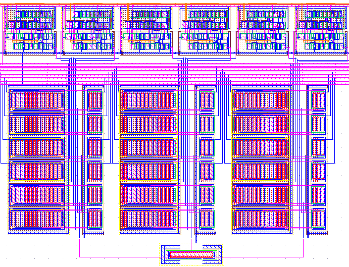
Fig. 1: Screenshot of the layout of the array unit-cell.