
 |
|
||||
BiographyFelix Johann Stampfl was born in 1994 in Austria and studied Technical Physics at the Technische Universität Graz, where he received his Diplom-Ingenieur degree (MSc equivalent) in 2023. Felix joined the Institute for Microelectronics in September 2023, where he is working towards his doctoral degree focusing on single defects in semiconductor devices while also being part of the CD-Lab for SDS team. |
|||||
CV Characterization of Si/SiGe Heterostructures at Low Temperature
Si/SiGe heterostructures have emerged as a promising technology for hosting qubits due to their compatibility with existing CMOS technology and their ability to support long-lived electron spins, essential for quantum information processing. A significant aspect of our research is the analysis of defects at the Si/SiO2 interface at a temperature of T = 4 K. These defects become filled through tunneling processes, leading to non-equilibrium conditions and anomalous behaviors in electrical measurements. Understanding these defects is crucial for improving the performance and reliability of quantum devices. We employ capacitance-voltage (CV) measurements at cryogenic temperatures to analyze how different device layers become populated by carriers during various operating stages. This analysis provides valuable insights into the distinct phases of carrier population and the impact of defects on device performance.
One of the key experimental topics we explore is the impact of varying the maximum gate voltage (VG,max) on the CV characteristics of the devices. The findings demonstrate that larger steps in threshold voltage shifts are observable at certain VG,max values, as shown in Fig.1, corresponding to the formation of the SiCap channel. This analysis is crucial for understanding the device dynamics and the influence of gate voltage on carrier population and defect behavior. By examining the CV characteristics at different VG,max values, we get a detailed understanding of how the gate voltage affects the carrier population and the overall performance of the device.
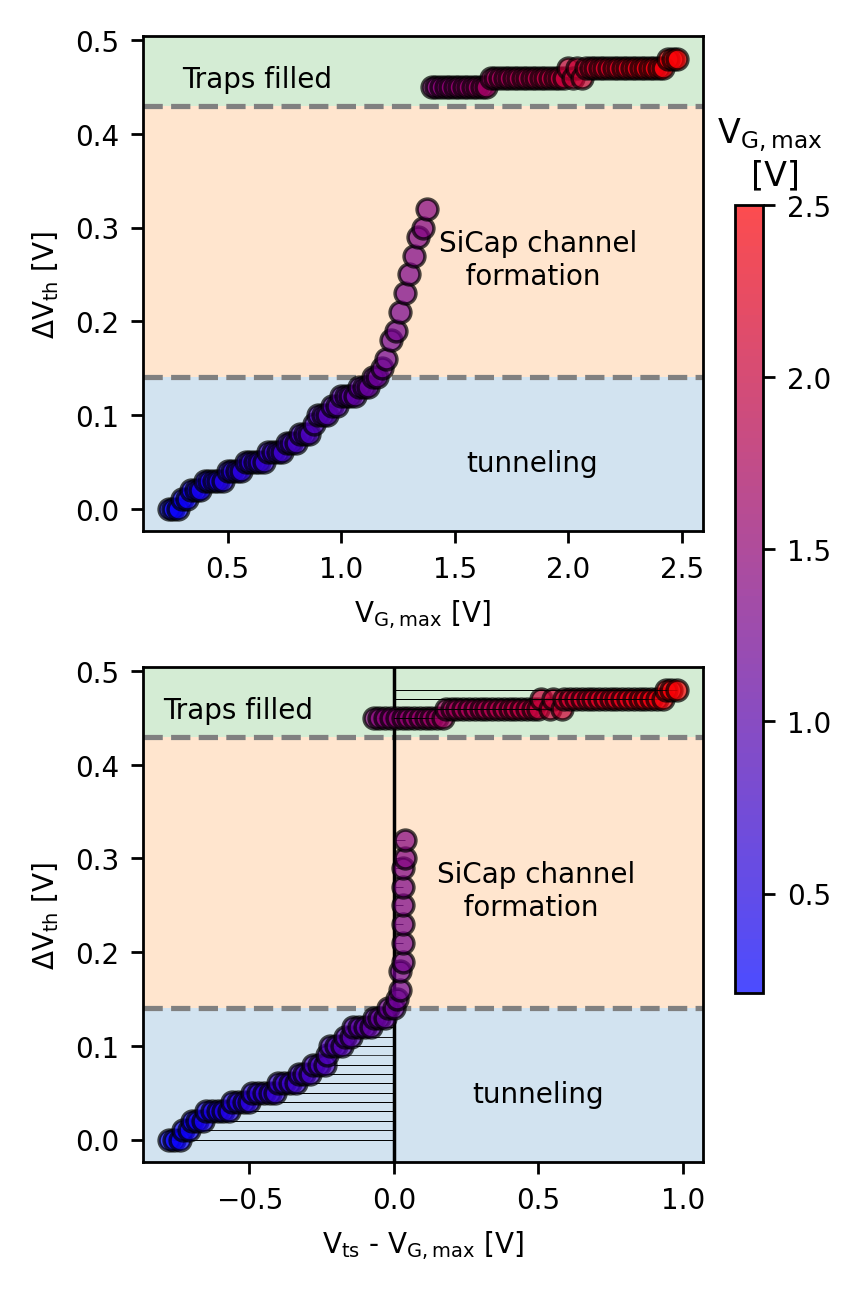
Fig. 1: Top: Threshold voltage hysteresis ∆Vth in dependence of VG,max. Bottom: ∆Vth in dependence of the difference in the SiCap threshold voltage Vts and VG,max with Vts,i = Vts - ∆Vth,i. The primary hysteresis increase happens then when VG,max is close to Vts,i.