
 |
|
||||
BiographyFrâncio Souza Berti Rodrigues was born in 1991 in Caxias do Sul, Brazil. He received his Bachelor's degree in Engineering Physics from the Federal University of Rio Grande do Sul (BSc, 2015). Subsequently, he received his Master's Degree in Microelectronics Manufacturing from the same university (MSc, 2018). After finishing his studies, he worked in research and development for the packaging industry before joining the Institute for Microelectronics in September 2019. He is currently pursuing his doctoral degree, researching high performance numerical approaches for Technology CAD within the scope of the Christian Doppler Laboratory for High Performance TCAD. |
|||||
Feature-Scale Modeling of Dry Etching in a Fluorocarbon Plasma
As semiconductor device performance continues to improve, fabrication technologies must advance accordingly. Among the most difficult steps in the fabrication process is plasma etching, which faces significant challenges for the creation of dense structures with high aspect ratios. Given the complexity of plasma etching, extensive empirical studies are often necessary, when developing new fabrication techniques. To support manufacturing progress and streamline this process, it is important to have precise, efficient, and predictive models of dry etching which can serve as virtual prototyping tools.
We implemented a TCAD workflow (see Fig. 1) for feature-scale dry etching in a fluorocarbon plasma within Silvaco's Victory Process simulation tool. To achieve this, we utilized a bottom-up ray tracer to calculate chemical species’ fluxes on various geometries and their source distributions. These fluxes serve as the input to a Langmuir kinetics coverage equation set which describes surface chemistry mechanisms and outputs local substrate etching or polymer deposition rates. The set of equations considers different mechanisms, including physical sputter etching, chemical etching, reactive ion etching, and polymer deposition. To apply the etch or deposition rates to the entire surface, we used a level set engine which updates the topography using a signed distance function accordingly.
We have applied our methodology to model a highly selective (SiO2 over Si) CF4/C4F8 plasma chemistry to form high aspect ratio structures, while using Ru metal as mask layers. We ran the simulation for a total etch time of 94 s, achieving the profile shown in Fig. 2 (b). The etch rate for SiO2 (332 nm/min) and the selectivity of SiO2/Ru (78) are within 3% of the experimentally reported values. The simulated trench-critical dimensions were also in excellent agreement: The depth (520 nm), width at trench bottom (58 nm), and width at half-depth (84 nm) are all within 5% of the experimental results. In Fig. 3 the result from the same process into a 3D array is displayed, showing the capability of generating larger 3D topographies which can serve as input for future device or process simulation procedures. In addition to its versatility for use with various materials and etching reactants, this workflow can serve as input for device simulators and is a cost-effective and efficient tool for optimizing plasma etching processes and generating process-aware 3D topographies.
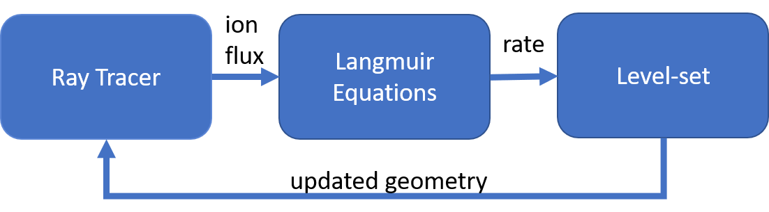
Fig. 1: The TCAD workflow is depicted in the flow diagram. At the beginning of the workflow, the ray tracer evaluates the flux of incoming species. Then, the Langmuir model evaluates the etch or deposition rates for each surface element. Finally, the level set engine applies the rates and updates the geometry accordingly.
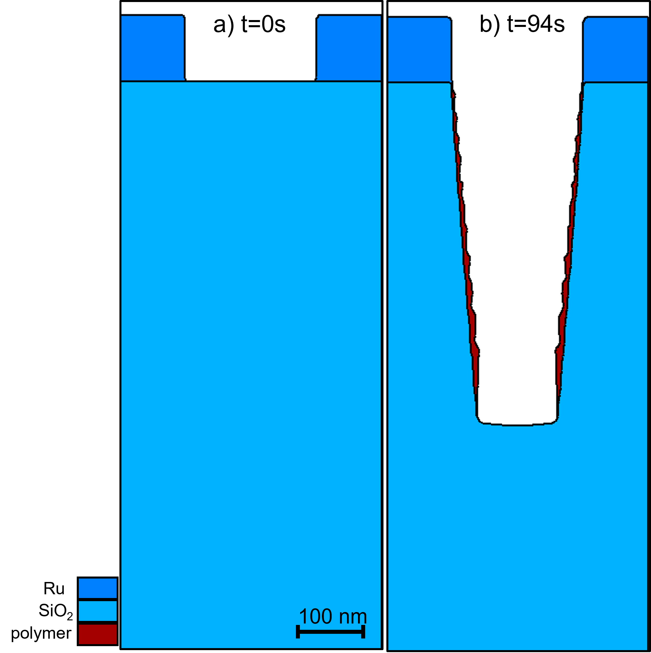
Fig. 2: (a) Two-dimensional (2D) cross-section of the initial feature shape with a 200 nm opening and a Ru mask height of 100 nm. (b) 2D cross-section after a total etch time of 94 s with the protective polymer layer, which is necessary for anisotropic structures.
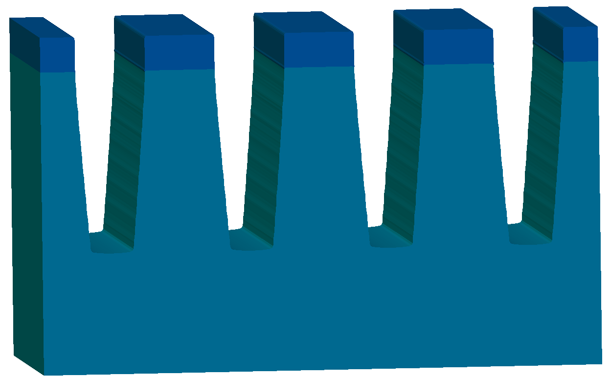
Fig. 3: By mirroring the final profile and stripping the polymer layer, we created a three-dimensional (3D) array of trenches, which demonstrates the potential of our methodology to generate complete 3D structures based on physical simulations; the geometries can subsequently be used in further TCAD process and device simulations.