C. MESFET Operation
To understand the operation of a MESFET, we consider the section under the gate of Fig. 4.36, as shown
in the left side of Fig. C.1. The source is grounded, the gate is zero or reverse biased, and the
drain is zero or forward biased; that is,
 and
and
 .
.
Figure C.1:
Cross section of the channel region of a MESFET (left), and drain voltage variation along the
channel (right).
|
|
The resistance of the channel is given by (3.127)
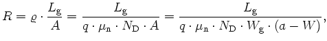 |
(C.1) |
where
 is the donor concentration,
  is the cross-section area of the current
flow and equals
is the cross-section area of the current
flow and equals
 , and
, and  is the average width
 of the
depletion region of the Schottky barrier.
of the
depletion region of the Schottky barrier.
When no gate voltage is applied and
 is small, a small current flows in the channel. The magnitude of the current is
given by
is small, a small current flows in the channel. The magnitude of the current is
given by
 . Therefore, the current varies linearly with the drain voltage. Of
course for any given drain voltage, the voltage along the channel increases from zero at the
source to
at the drain. Thus, the Schottky barrier becomes increasingly reverse
biased as we proceed from the source to the drain. As
is increased,
increases, and the average cross-sectional area for the current flow is reduced. The channel
resistance
. Therefore, the current varies linearly with the drain voltage. Of
course for any given drain voltage, the voltage along the channel increases from zero at the
source to
at the drain. Thus, the Schottky barrier becomes increasingly reverse
biased as we proceed from the source to the drain. As
is increased,
increases, and the average cross-sectional area for the current flow is reduced. The channel
resistance  also increases. As a result, the current increases at a slower rate.
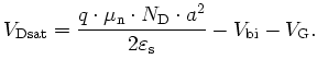
As the drain voltage further increases, eventually the depletion region touches the
semi-insulating substrate. That happens when  at the drain. We can obtain the
corresponding value of the drain voltage, called the saturation voltage
at the drain. We can obtain the
corresponding value of the drain voltage, called the saturation voltage
 ,
from
,
from
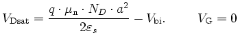 |
(C.2) |
At this drain voltage, the source and the drain are pinched off or completely separated
by a reverse-biased depletion region. At this point, a large drain current called the
saturation current
 can flow across the depletion region. Beyond this
pinch-off point, as
can flow across the depletion region. Beyond this
pinch-off point, as
 , the current remains essentially at the value
and is independent of
.
, the current remains essentially at the value
and is independent of
.
When a gate voltage is
applied to reverse bias the gate contact, the depletion-layer width increases. For small
, the channel again acts as a resistor but its resistance is higher because the
cross-section area available for current flow is decreased. When
is increased
to a certain value, the depletion region again touches the semi-insulating substrate. The value
of this
is given by
 |
(C.3) |
For an n-channel MESFET, the gate voltage is negative with respect to the source, so we use
the absolute value of
 in (C.3). One can see from (C.3) that
the application of a gate voltage
reduces the drain voltage required for the
onset of pinch-off by an amount equal to
.
in (C.3). One can see from (C.3) that
the application of a gate voltage
reduces the drain voltage required for the
onset of pinch-off by an amount equal to
.
Subsections
T. Ayalew: SiC Semiconductor Devices Technology, Modeling, and Simulation
![\includegraphics[width=0.50\linewidth]{figures/mesfet-b.eps}](img835.png)
![\includegraphics[width=0.46\linewidth]{figures/mesfet-c.eps}](img836.png)