|
|
|
|
Previous: 3.3.1 Low-Field Carrier Mobility Up: 3.3 Carrier Mobility Next: 3.3.3 High-Field Mobility and Velocity Saturation |
|
|
|
|
Previous: 3.3.1 Low-Field Carrier Mobility Up: 3.3 Carrier Mobility Next: 3.3.3 High-Field Mobility and Velocity Saturation |
 |
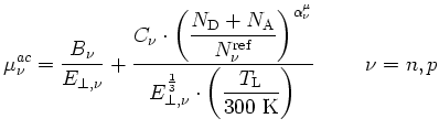
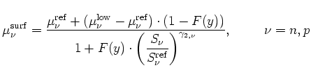
(3.86) |
 |
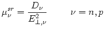
(3.87) |
![$\displaystyle \mu_{\nu}^\mathrm{cc}= \frac {D\cdot\left(\displaystyle\frac{T_\m...
...\ K}}\right)^2\cdot(p\cdot n)^{-\frac{1}{3}}\right)\right]\hspace{1cm}\nu = n,p$](img433.png)
![$\displaystyle \mu^\mathrm{tot}_{\nu} = \left[\frac {1}{\mu^{b}_{\nu}} + \frac {1}{\mu^{ac}_{\nu}} + \frac {1}{\mu^{sr}_{\nu}}\right]^{-1}. \hspace{1cm}\nu = n,p$](img442.png)