Next: 5.2.2 Simulation and Parameter Up: 5.2 Parameter Extraction of Previous: 5.2 Parameter Extraction of Contents
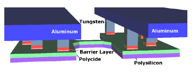
A typical structure of a fuse consisting of various interconnect materials is shown in Figure 5.11, where the complex material composition is presented. To use interconnect materials only is advantageous because additional costs due to extra layers, masks, and process steps can be minimized by using already available materials and process steps. Moreover, in terms of power and area consumption, fuses which are made of already available interconnect materials are economically more attractive compared to hybrid technologies [340] which have to use different materials and thus additional process steps.
Because the downscaling process demands also decreased supply voltages, a careful design is required which includes a rigorous optimization of the fusing structure to ensure the reliability of the programming mechanism [342] and to minimize the power consumption during the programming process of the fuse.
Since the fusing mechanism takes place within a very short time (couple of
![]() ns) for an ideal voltage step and several micro seconds for a voltage ramp
measurements are hard to obtain [90].
ns) for an ideal voltage step and several micro seconds for a voltage ramp
measurements are hard to obtain [90].
A better insight into the electrical and thermal characteristics is desired for the
materials used in the fusing structure as shown in Figure 5.11.
In particular, the goal of the parameter extraction is the characteristics of
the temperature dependence of the thermal and the electrical conductivity of the
key materials polySi and the polycide (
![]() ).
In order to obtain reasonable results from the simulation accurate information
about of the test circuit for the fusing device is
required [47].
).
In order to obtain reasonable results from the simulation accurate information
about of the test circuit for the fusing device is
required [47].
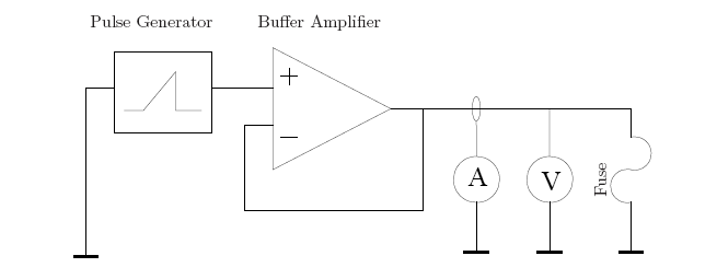
Because the measurement of the programming mechanism has to be carried out
within a certain amount of nanoseconds, the programming is artificially
prolongated to a couple of microseconds for the fusing time by applying a
voltage ramp with a rising period of ![]() s. This procedure allows to
measure the fusing current with reasonable accuracy.
The corresponding measurement set up is shown in Figure 5.12, where a
voltage ramp is applied to a buffer amplifier to minimize the influence
(impedance) of the function generator and to provide a high slew rate.
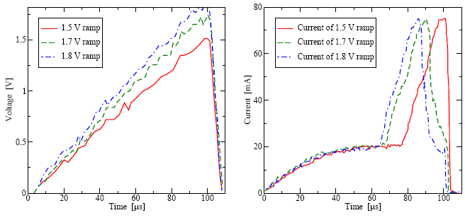
The resulting measurements are shown in Figure 5.13.
These measurements serve as reference data for the
parameter identification procedure.
s. This procedure allows to
measure the fusing current with reasonable accuracy.
The corresponding measurement set up is shown in Figure 5.12, where a
voltage ramp is applied to a buffer amplifier to minimize the influence
(impedance) of the function generator and to provide a high slew rate.
The resulting measurements are shown in Figure 5.13.
These measurements serve as reference data for the
parameter identification procedure.