Next: 6.4 Outlook Up: 6. Conclusions Previous: 6.2 Multiple (Thermal) Redundancy Contents
As the last decades have shown, the progress in semiconductor technology seems to continue unabatedly. In the past, despite of the forecast red brick walls, the only constant factor and a simultaneously self-fulfilling prophecy was Gordon E. MOORE's law, which is likely to remain valid for the next decade. However, there are apprehensions about physical size and other constraints but similar concerns were announced the last decades ago. With the present technologies the industry is facing similar problems as ten or twenty years ago. However, progress through innovation is the only way to succeed in economics as well as in science and technology. Therefore, alternatives are investigated where some of which are looking more promising than others. One among these auspicious technologies is the use of new devices made of or supported by carbo-nano-tubes (CNT). They offer extreme values for the electrical and thermal conductivities but, on the other hand, show major difficulties in fabrication and embedding into existing systems, for instance with respect to contacting the CNTs. However, in nearly every conference on nano technology additional steps towards the usability of CNTs are presented. Thus, it is only a matter of time that such devices will be available the leaders in the sector of advanced semiconductors.
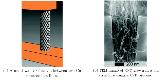
As proposed in [347], CNTs have already been used in interconnects for prototypes Figure 6.1. This may overcome or even solve critical problems with the conductivity and adhesion of Cu, which is related to electro-migration. By using CNTs in the vias, their advantageous properties can be used to increase reliability rather than with the expensive production of protective barrier coatings.
 |