Using the first design step, i.e. the effect of
ELDs, it was demonstrated that the transmission of electrons around
the Fermi level can be increased (from
![]() to
to
![]() and
and
![]() in the
presence of one and two ELDs, respectively). An asymmetry is thus
created between holes and electrons. This increases both the
conductance and the Seebeck coefficient of the channel as shown in
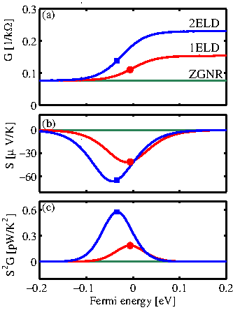
Fig. 3.27. Figure 3.27-a
shows the conductance of the 2ELD-ZGNR(8,4,8) (blue), of the ELD-ZGNR
(10,10) (red), and of the pristine nanoribbon (green) at
in the
presence of one and two ELDs, respectively). An asymmetry is thus
created between holes and electrons. This increases both the
conductance and the Seebeck coefficient of the channel as shown in
Fig. 3.27. Figure 3.27-a
shows the conductance of the 2ELD-ZGNR(8,4,8) (blue), of the ELD-ZGNR
(10,10) (red), and of the pristine nanoribbon (green) at ![]() . As expected, the conductance of the channel with
two ELDs is the largest, followed by the channel with one ELD. The conductances
are larger than that of the pristine channel by
. As expected, the conductance of the channel with
two ELDs is the largest, followed by the channel with one ELD. The conductances
are larger than that of the pristine channel by ![]() and
and ![]() ,
respectively. Figure 3.27-b shows the changes of
the Seebeck coefficient after the introduction of the ELDs in the
nanoribbon. Due to its metallic behavior and the flat transmission near the Fermi level, the pristine channel exhibits zero Seebeck coefficient. Due to the asymmetry built up after the introduction of the ELDs, however, the Seebeck coefficient increases for both
channels. The channel with two line defects has the largest asymmetry,
and therefore the largest Seebeck coefficient (in absolute
values). Finally, the power factor in Fig. 3.27-c
is indeed largely improved in the ELD structures, and
especially the 2ELD-ZGNR channel.
,
respectively. Figure 3.27-b shows the changes of
the Seebeck coefficient after the introduction of the ELDs in the
nanoribbon. Due to its metallic behavior and the flat transmission near the Fermi level, the pristine channel exhibits zero Seebeck coefficient. Due to the asymmetry built up after the introduction of the ELDs, however, the Seebeck coefficient increases for both
channels. The channel with two line defects has the largest asymmetry,
and therefore the largest Seebeck coefficient (in absolute
values). Finally, the power factor in Fig. 3.27-c
is indeed largely improved in the ELD structures, and
especially the 2ELD-ZGNR channel.
|
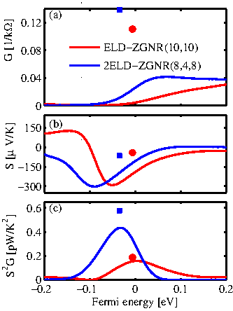
In Figure 3.28 the same thermoelectric
coefficients for the same structures as in
Fig. 3.27 are shown, but now edge roughness and positive
impurities are included in the calculation. The length of the channels
in this case is
![]() . A similar qualitative behavior is observed
as in Fig. 3.27 for both
channels. Quantitatively, however, the conductance in
Fig. 3.28-a is now significantly reduced by a
factor of
. A similar qualitative behavior is observed
as in Fig. 3.27 for both
channels. Quantitatively, however, the conductance in
Fig. 3.28-a is now significantly reduced by a
factor of ![]() (the dots correspond to the position of the peak
of the power factor of the devices without roughness and impurities in
Fig. 3.27). The Seebeck coefficient in
Fig. 3.28-b, on the other hand
increases. Finally, the peak of the power factor in
Fig. 3.28-c reduces only slightly compared to the
peak of the power factor of the devices without edge roughness in
Fig. 3.27-c (dots).
(the dots correspond to the position of the peak
of the power factor of the devices without roughness and impurities in
Fig. 3.27). The Seebeck coefficient in
Fig. 3.28-b, on the other hand
increases. Finally, the peak of the power factor in
Fig. 3.28-c reduces only slightly compared to the
peak of the power factor of the devices without edge roughness in
Fig. 3.27-c (dots).
|
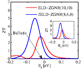
For the devices that include
rough edges, however, as demonstrated in
Fig. 3.26, the phonon thermal conductivity is
drastically reduced compared to the electronic thermal conductivity. A
large improvement in ![]() is therefore expected. Figure 3.29 shows
is therefore expected. Figure 3.29 shows ![]() versus
energy at room temperature for the ELD-ZGNR(10,10), the
ELD-ZGNR(10,10) with impurities and roughness (red), and the
2ELD-ZGNR(8,4,8) (blue) with impurities and roughness. As indicated,
large values of
versus
energy at room temperature for the ELD-ZGNR(10,10), the
ELD-ZGNR(10,10) with impurities and roughness (red), and the
2ELD-ZGNR(8,4,8) (blue) with impurities and roughness. As indicated,
large values of ![]() can be achieved, especially in the case of the
device with two ELDs. The phonon lattice conductivity value used in
this calculation was extracted using the MFP method. As
explained in Sec. 3.3.4, that value could be
can be achieved, especially in the case of the
device with two ELDs. The phonon lattice conductivity value used in
this calculation was extracted using the MFP method. As
explained in Sec. 3.3.4, that value could be ![]() lower than the value
extracted from direct integration of the simulated phonon transmission. In the
inset of Fig. 3.29 the
lower than the value
extracted from direct integration of the simulated phonon transmission. In the
inset of Fig. 3.29 the ![]() versus energy using the
versus energy using the
![]() values extracted from the transmission are shown. Indeed
the values might be reduced by a factor of
values extracted from the transmission are shown. Indeed
the values might be reduced by a factor of ![]() , but still peak
, but still peak
![]() values above 2 can be achieved at room temperature, which is
comparable and even better than the best thermoelectric materials to
date [96]. It is worth mentioning that as shown by Ref. [19]
rough ZGNRs can have high
values above 2 can be achieved at room temperature, which is
comparable and even better than the best thermoelectric materials to
date [96]. It is worth mentioning that as shown by Ref. [19]
rough ZGNRs can have high ![]() values even without the presence of
ELDs. For this the asymmetry in the sharp edges of the higher
subbands is utilized at energies above
values even without the presence of
ELDs. For this the asymmetry in the sharp edges of the higher
subbands is utilized at energies above
![]() . Those
energies however, are too high and can not easily be reached. Finally
it is necessary to mention here that the formalism has considered scattering only by
edge roughness and impurity scattering, whereas phonon scattering and
dephasing mechanisms are not included. However, as it is shown for 1D
nanowires [97], the effects of impurity scattering and edge
roughness are the most important scattering effects in channels of
cross sections below
. Those
energies however, are too high and can not easily be reached. Finally
it is necessary to mention here that the formalism has considered scattering only by
edge roughness and impurity scattering, whereas phonon scattering and
dephasing mechanisms are not included. However, as it is shown for 1D
nanowires [97], the effects of impurity scattering and edge
roughness are the most important scattering effects in channels of
cross sections below
![]() , and one can expect this to hold also for GNRs
as well.
, and one can expect this to hold also for GNRs
as well.
|