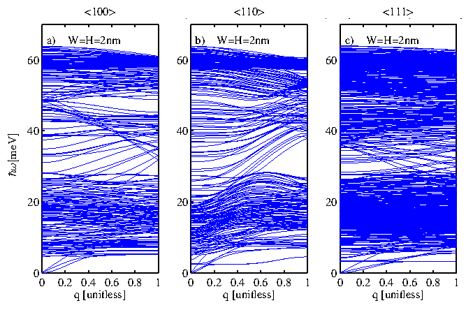
The phononic dispersions of silicon nanowires of
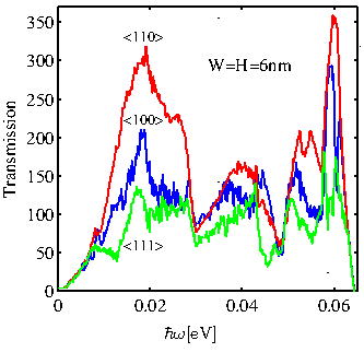
![]() cross section for different transport orientations are shown in Fig. 4.1. There are differences in the dispersions, especially in the low energy, low momentum region, which indicate that the thermal properties could be orientation-dependent as well. Figure 4.2 shows the ballistic transmission function of nanowires with side sizes
cross section for different transport orientations are shown in Fig. 4.1. There are differences in the dispersions, especially in the low energy, low momentum region, which indicate that the thermal properties could be orientation-dependent as well. Figure 4.2 shows the ballistic transmission function of nanowires with side sizes
![]() for three orientations. The transmission function of the
for three orientations. The transmission function of the
![]() nanowires is the highest in most part of the energy spectrum, whereas the transmission of the
nanowires is the highest in most part of the energy spectrum, whereas the transmission of the
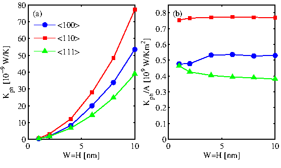
![]() nanowires is the lowest in almost the entire energy spectrum. As a result, the ballistic lattice thermal conductance of the nanowires (see Fig. 4.3-a) shows that the
nanowires is the lowest in almost the entire energy spectrum. As a result, the ballistic lattice thermal conductance of the nanowires (see Fig. 4.3-a) shows that the
![]() nanowires has the highest thermal conductance compared to the
nanowires has the highest thermal conductance compared to the
![]() and
and
![]() nanowires.
nanowires.
|
The thermal conductance is larger for the
![]() nanowires of all the side sizes we have considered, up to
nanowires of all the side sizes we have considered, up to
![]() as shown in Fig. 4.3-a. The difference between the thermal conductances of the
as shown in Fig. 4.3-a. The difference between the thermal conductances of the
![]() nanowire, which has the highest, and the
nanowire, which has the highest, and the
![]() nanowire which has the lowest, is a factor of
nanowire which has the lowest, is a factor of ![]() . Another observation is that the thermal conductance increases as the cross section of the nanowire increases. This is expected since the larger nanowires contain more transport modes. The increase is close to linear. Once the conductances are normalized by the cross section area of the nanowires, however, the resultant normalized conductances remain almost constant. This is indicated in the Fig. 4.3-b. In this case, again, the
. Another observation is that the thermal conductance increases as the cross section of the nanowire increases. This is expected since the larger nanowires contain more transport modes. The increase is close to linear. Once the conductances are normalized by the cross section area of the nanowires, however, the resultant normalized conductances remain almost constant. This is indicated in the Fig. 4.3-b. In this case, again, the
![]() nanowire has clearly the lowest conductivity, almost 2 times lower than the
nanowire has clearly the lowest conductivity, almost 2 times lower than the
![]() nanowire for all cross section sizes. In the next section, the reasons behind the anisotropy of the thermal conductance and conductivity are elucidated in terms of the nanowires’ phonon bandstructure and its related quantities.
nanowire for all cross section sizes. In the next section, the reasons behind the anisotropy of the thermal conductance and conductivity are elucidated in terms of the nanowires’ phonon bandstructure and its related quantities.
|
|