Before a device simulation can be started, the contacts of the
device have to be defined, since these contacts represent the
geometric position of the electrical boundary conditions. The
simulator must know a unique name of each contact to identify it
during the device simulation in order to set the boundary conditions
(potential, current, parasitic values, work function etc.) appropriately.
To enable an automatic generation of these contact names, the names
have to be defined in the device layout. These regions have to be
projected on the final two- or three-dimensional structure in a
post processing step of the results of the process-simulation. If the
contact naming follows a certain nomenclature, standard device
simulator templates for certain semiconductor devices can be used
automatically. If, for instance, every source, drain and gate of a CMOS
transistor is named source,drain and gate consistently
in every layout, a standard template for the device simulator command
file can be used to extract electrical parameters, like threshold, saturation
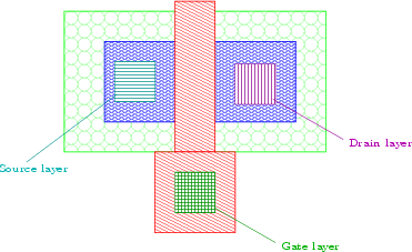
current, etc. This naming is performed by using the CONTACT layer data, to identify
the different contacts. For this purpose some selected contact structures are
copied to the corresponding contact naming layers like source,
drain, gate etc.
An example of such a naming approach is shown in Figure 3.11.