Previous: 3.1.2 Mobility Up: 3.1 Transport Physics Considered for Power Semiconductor Devices Next: 3.1.4 Carrier Lifetime
Recombination and generation of electrons and holes is a process by which both carriers are either created or destroyed.
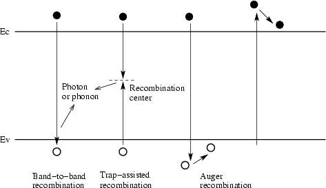
Figure 3.2 shows the most important recombination mechanisms. Excess carriers decay by these recombination processes, and the energy of carriers must be dissipated during this process by several ways, such as emission of a photon, heat generation in the lattice in the form of phonons, and the transmission of the energy to a third particle.
As shown in the figure, band-to-band recombination occurs when an electron falls from its conduction band state into the empty valence band state associated with a hole. It releases its energy in the form of light (a photon). Because silicon has an indirect band gap structure the probability of this direct transition is small.
Trap-assisted recombination is a two-step process. It occurs when an electron falls into a trap, an energy level within the bandgap caused by the presence of a foreign atom or a structural defect. Once the trap is filled it cannot accept another electron. The electron occupying the trap, in a second step, falls into an empty valence band state. It significantly changes the momentum of indirect semiconductors. The statistics of this recombination process were treated for the first time by Shockley, Read, and Hall (SRH). They took a single level recombination center in the band gap into account. SRH recombination and generation process involves four steps, such as electron capture, hole capture, electron emission and hole emission. (3.14) shows the mathematical model of the SRH recombination and generation rate
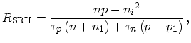 |
(3.14) |
 |
(3.15) |
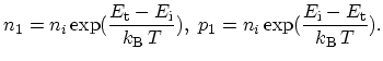
where ![]() and
and ![]() are the electron and hole minority carrier lifetimes in heavily
doped
are the electron and hole minority carrier lifetimes in heavily
doped ![]() - and
- and ![]() - type silicon,
- type silicon,
![]() and
and
![]() are the intrinsic and recombination levels,
respectively. In the derivation of the SRH recombination generation model it is
assumed that the number of trap centers is much larger than that of the
carriers involved in this process.
are the intrinsic and recombination levels,
respectively. In the derivation of the SRH recombination generation model it is
assumed that the number of trap centers is much larger than that of the
carriers involved in this process.
Another important effect for the modeling of MOS structures is the surface recombination.
Since the semiconductor surface and interface between the semiconductor and
the insulating material contain a large number of defects, such as dangling bonds,
recombination centers at the semiconductor surface and interface can have a significant
impact on the behavior of devices.
The surface recombination model for the numerical simulation can be
modeled by the SRH recombination equation.
The only difference compared to the bulk recombination is that the recombination
is due to a two-dimensional density
of traps,
![]() , as the traps only exist at the surface or interface.
, as the traps only exist at the surface or interface.
Auger recombination
![]() involves three particles: an electron and a hole, which recombine
in a band-to-band transition and give off the resulting energy to another electron
or hole. The expression for the net recombination rate is similar to that of
simple band-to-band recombination, but the involvement of a third particle
affects the recombination rate:
involves three particles: an electron and a hole, which recombine
in a band-to-band transition and give off the resulting energy to another electron
or hole. The expression for the net recombination rate is similar to that of
simple band-to-band recombination, but the involvement of a third particle
affects the recombination rate:
| (3.16) |
Jong-Mun Park 2004-10-28