Previous: 3.3.1 Standard Power MOSFETs Up: 3.3 Super-Junction Concepts Next: 3.3.3 Vertical SJ DMOSFETs
The SJ concept is based on the idea to achieve charge balance during the
off-state between alternatively stacked ![]() - and
- and ![]() -regions (pillars).
The stacks can be made vertically and (or) laterally.
In the off-state the
-regions (pillars).
The stacks can be made vertically and (or) laterally.
In the off-state the ![]() - and
- and ![]() -pillars is completely depleted
before breakdown, and the electric field distribution becomes flat in the
depletion region.
This causes a linear relationship between
-pillars is completely depleted
before breakdown, and the electric field distribution becomes flat in the
depletion region.
This causes a linear relationship between
![]() and BV instead of the power relationship in (3.39).
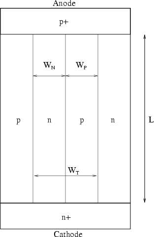
Figure 3.14 shows a schematic view of the SJ diode. With alternating
and BV instead of the power relationship in (3.39).
Figure 3.14 shows a schematic view of the SJ diode. With alternating
![]() - and
- and ![]() -columns
in the drift region the doping in this region can be increased drastically.
In the off-state, increased cathode bias first extends the depletion
layer of the
-columns
in the drift region the doping in this region can be increased drastically.
In the off-state, increased cathode bias first extends the depletion
layer of the ![]() - and
- and ![]() -column junction in the horizontal direction, and both
-column junction in the horizontal direction, and both
![]() - and
- and ![]() -columns are completely depleted at a larger cathode voltage.
-columns are completely depleted at a larger cathode voltage.
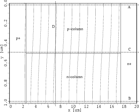
Figure 3.15 shows the potential distribution of the SJ ![]() -diode at a reverse voltage
of 300V. Potential lines are uniformly distributed throughout the drift region.
This structure is designed to obtain a BV of 300V with an
-diode at a reverse voltage
of 300V. Potential lines are uniformly distributed throughout the drift region.
This structure is designed to obtain a BV of 300V with an
![]() - and
- and ![]() -column width
-column width
![]()
![]()
![]()
![]() 0.5
0.5![]() m
and drift length
m
and drift length
![]()
![]() 15
15![]() m.
With the SJ concept drift doping can be increased
by decreasing the pillar width. However, considering the built-in
depletion region, the width cannot be decreased indefinitely and
there exists a minimum pillar width which is comparable to the built-in
depletion width. Further decrease the pillar width below certain critical value
the pillar doping cannot be increased.
One can expect a square shape of the electric field distribution instead of the triangular
shape for the case of conventional
m.
With the SJ concept drift doping can be increased
by decreasing the pillar width. However, considering the built-in
depletion region, the width cannot be decreased indefinitely and
there exists a minimum pillar width which is comparable to the built-in
depletion width. Further decrease the pillar width below certain critical value
the pillar doping cannot be increased.
One can expect a square shape of the electric field distribution instead of the triangular
shape for the case of conventional ![]() -diodes.
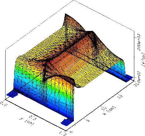
Figure 3.16 shows the electric field distribution of the SJ
-diodes.
Figure 3.16 shows the electric field distribution of the SJ ![]() -diode.
It shows a rather high electric field along the
-diode.
It shows a rather high electric field along the ![]() -junction
(and
-junction
(and ![]() - and
- and ![]() -junction) compared to that at each
side of the device, but the electric field distribution is nearly square
shaped throughout the drift region.
-junction) compared to that at each
side of the device, but the electric field distribution is nearly square
shaped throughout the drift region.
Because of the lateral ![]() - and
- and ![]() -column junction at the middle of the
drift region (and the thin layer thickness of each column), a large depletion region
can be observed at a relatively low voltage. For the conventional
-column junction at the middle of the
drift region (and the thin layer thickness of each column), a large depletion region
can be observed at a relatively low voltage. For the conventional ![]() -junction
diode the delpetion region expends gradually as the voltage increases.
Fot the SJ structure, on the other hand, relatively thin
-junction
diode the delpetion region expends gradually as the voltage increases.
Fot the SJ structure, on the other hand, relatively thin ![]() - and
- and ![]() -pillars
become completely depleted at a low voltage (about 10V in this example).
Although the doping concentrations of each column are much more higher compared
to that of the drift region for the conventional
-pillars
become completely depleted at a low voltage (about 10V in this example).
Although the doping concentrations of each column are much more higher compared
to that of the drift region for the conventional ![]() -diode,
it behaves similar to a lightly doped drift layer.
-diode,
it behaves similar to a lightly doped drift layer.
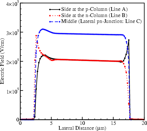
Figure 3.17 shows the electric field along the cut lines
A, B, and C. As expected from Figure 3.16 higher electric field
is observed along the ![]() - and
- and ![]() -pillar junction (cut line C), and peak electric fields are
observed at the
-pillar junction (cut line C), and peak electric fields are
observed at the ![]() - and
- and ![]() -junction (peak positions at cut lines A and B).
Figure 3.18 shows
the electric field along the
-junction (peak positions at cut lines A and B).
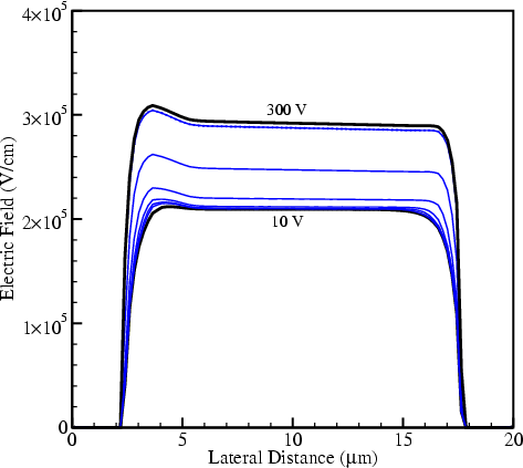
Figure 3.18 shows
the electric field along the ![]() -junction at the middle of the
device (cut line C in Figure 3.15) for reverse voltages from 10V to
300V, and it is flat throughout the junction.
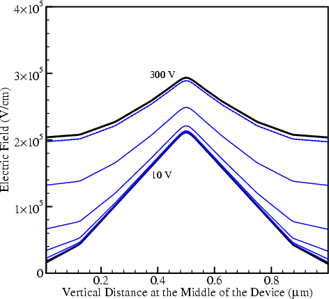
Figure 3.19 shows the electric field at the vertical direction of
the device (along the cut line D in Figure 3.15). High electric
field for each voltage step is observed at the middle of the cut line,
and the voltage difference between the middle and the side of the structure
becomes lower at high reverse voltage.
Even at a low applied voltage of 10V, one can see a fairly high electric field at
the side of each column because of the fully
depleted
-junction at the middle of the
device (cut line C in Figure 3.15) for reverse voltages from 10V to
300V, and it is flat throughout the junction.
Figure 3.19 shows the electric field at the vertical direction of
the device (along the cut line D in Figure 3.15). High electric
field for each voltage step is observed at the middle of the cut line,
and the voltage difference between the middle and the side of the structure
becomes lower at high reverse voltage.
Even at a low applied voltage of 10V, one can see a fairly high electric field at
the side of each column because of the fully
depleted ![]() - and
- and ![]() -columns.
-columns.
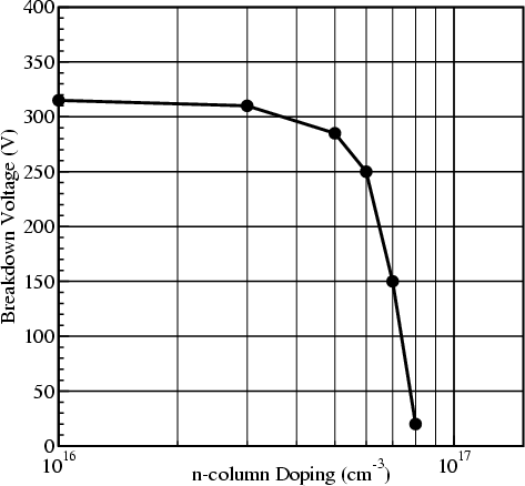
Figure 3.20 shows the BV versus drift doping concentration.
The ![]() - and
- and ![]() -column doping
concentration over the critical value will reduce the BV of the device abruptly.
-column doping
concentration over the critical value will reduce the BV of the device abruptly.
 |
 |
 |
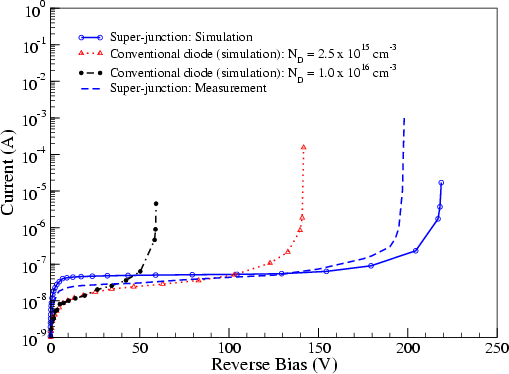 |
Figure 3.21 shows the BV comparison for the SJ and conventional ![]() -diodes.
Drift length of the
-diodes.
Drift length of the ![]() -diode is
-diode is
![]()
![]() 9.5
9.5![]() m. SJ
m. SJ ![]() -diode is built in
-diode is built in
![]() - and
- and ![]() -column width of 1.0
-column width of 1.0![]() m and 3.0
m and 3.0![]() m, respectively,
and
m, respectively,
and ![]() - and
- and ![]() -column doping of 1.0
-column doping of 1.0 ![]()
![]()
![]() and
3.3
and
3.3 ![]()
![]()
![]() , respectively. For the simulation of SJ
, respectively. For the simulation of SJ
![]() -diode complete charge balance of the drift region was assumed, this can be the
major reason that the simulated BV is a little higher than the measured data.
Because of the reduced drift length with high doping concentration in the drift region,
conventional
-diode complete charge balance of the drift region was assumed, this can be the
major reason that the simulated BV is a little higher than the measured data.
Because of the reduced drift length with high doping concentration in the drift region,
conventional ![]() -diodes (drift region doping concentration
of 2.5
-diodes (drift region doping concentration
of 2.5 ![]()
![]()
![]() and 1.0
and 1.0 ![]()
![]()
![]() , respectively)
have lower breakdown voltages compared to the SJ
, respectively)
have lower breakdown voltages compared to the SJ ![]() -diode.
-diode.