Previous: 3.3.3 Vertical SJ DMOSFETs Up: 3.3 Super-Junction Concepts Next: 4. Case Study
Previous sections showed that SJ structures result in a uniform electric field distribution in the drift region. This gives the highest possible BV for a given drift region length because of the flat shape of the electric field instead of the triangular shape, independent of the doping concentration of the pillars. Hence, significant improvement in the specific on-resistance is achieved by using high doping concentrations in the drift region.
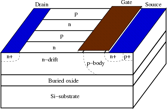
In the case of a dielectrically isolated SJ LDMOSFET implemented
on an SOI substrate, three-dimensional RESURF action
can be expected in the off-state. Figure 3.24 shows such a SJ SOI-LDMOSFET.
Like the vertical SJ DMOSFET the ![]() - and
- and ![]() -pillars
in the drift region must be completely depleted before breakdown.
In addition, a large amount of voltage drops in the buried oxide like
in a conventional SOI-LDMOSFET.
-pillars
in the drift region must be completely depleted before breakdown.
In addition, a large amount of voltage drops in the buried oxide like
in a conventional SOI-LDMOSFET.
By using a relatively thin SOI layer for the starting material, complicated
multiple epitaxial deposition can be eliminated and additional
implantation steps can be used to form the ![]() - and
- and ![]() -columns
on an SOI. For the case of medium-voltage SJ SOI-LDMOSFETs the charge of
the
-columns
on an SOI. For the case of medium-voltage SJ SOI-LDMOSFETs the charge of
the ![]() -body also affects the RESURF condition significantly.
In Chapter 4 we will show detailed three-dimensional simulations for
our SJ SOI-LDMOSFETs.
-body also affects the RESURF condition significantly.
In Chapter 4 we will show detailed three-dimensional simulations for
our SJ SOI-LDMOSFETs.
Jong-Mun Park 2004-10-28